SLVAEM2A January 2020 – March 2021 TPS3700-Q1
4.2 DSE Package
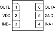
Figure 4-2 shows the TPS3700-Q1 pin diagram for the DSE package. For a detailed description of the device pins please refer to the Pin Configuration and Functions section in the TPS3700-Q1 data sheet.
 Figure 4-2 Pin Diagram (DSE Package)
WSON-6
Top View
Table 4-6 Pin FMA for Device Pins
Short-Circuited to Ground
| Pin Name | Pin No. | Description of Potential Failure Effect(s) | Failure Effect Class |
|---|---|---|---|
| OUTB | 1 | No damage to device, overvoltage output pin nonfunctional, OUTB indicates an overvoltage fault, increase in system current due to current through OUTB pull-up resistor | B |
| VDD | 2 | No damage to device, but device is unpowered. Device is nonfunctional. | B |
| INB- | 3 | No damage to device, overvoltage sense input pin nonfunctional, OUTB indicates no overvoltage fault. | B |
| INA+ | 4 | No damage to device, undervoltage sense input pin nonfunctional, OUTA indicates undervoltage fault, increase in system current due to current through OUTA pull-up resistor | B |
| GND | 5 | Normal Operation. | D |
| OUTA | 6 | No damage to device, undervoltage output pin nonfunctional, OUTA indicates an undervoltage fault, increase in system current due to current through OUTA pull-up resistor | B |
Table 4-7 Pin FMA for Device Pins
Open-Circuited
| Pin Name | Pin No. | Description of Potential Failure Effect(s) | Failure Effect Class |
|---|---|---|---|
| OUTB | 1 | Open-drain output requires pull-up resistor to pull-up voltage for correct functionality. | B |
| VDD | 2 | No damage to device, but device is unpowered. Device is nonfunctional. | B |
| INB- | 3 | No damage to device, overvoltage sense input pin nonfunctional, OUTB indicates no overvoltage fault. | B |
| INA+ | 4 | No damage to device, undervoltage sense input pin nonfunctional, OUTA indicates undervoltage fault. | B |
| GND | 5 | No damage to device, but device is unpowered. Device is nonfunctional. | B |
| OUTA | 6 | Open-drain output requires pull-up resistor to pull-up voltage for correct functionality. | B |
Table 4-8 Pin FMA for Device Pins
Short-Circuited to Adjacent Pin
| Pin Name | Pin No. | Shorted to | Description of Potential Failure Effect(s) | Failure Effect Class |
|---|---|---|---|---|
| OUTB | 1 | VDD | Open-drain output requires pull-up resistor to pull-up voltage for correct functionality. OUTB indicates no overvoltage fault. OUTB shorted to VDD can violate the output current ABS MAX rating and cause damage if INB- is below V_IT- | A |
| VDD | 2 | INB- | No damage to device, overvoltage sense input pin nonfunctional, OUTB indicates overvoltage fault. | B |
| INB- | 3 | INA+ | No damage to device, device monitors a single input for both undervoltage and overvoltage | C |
| INA+ | 4 | GND | No damage to device, undervoltage sense input pin nonfunctional, OUTA indicates undervoltage fault, increase in system current due to current through OUTA pull-up resistor | B |
| GND | 5 | OUTA | No damage to device, undervoltage output pin nonfunctional, OUTA indicates an undervoltage fault, increase in system current due to current through OUTA pull-up resistor | B |
| OUTA | 6 | OUTB | No damage to device, device outputs a single signal for both undervoltage and overvoltage window monitoring. OUTA and OUTB indicate a fault if either undervoltage or overvoltage condition occurs | C |
Table 4-9 Pin FMA for Device Pins Short-Circuited to
VDD
| Pin Name | Pin No. | Description of Potential Failure Effect(s) | Failure Effect Class |
|---|---|---|---|
| OUTB | 1 | Open-drain output requires pull-up resistor to pull-up voltage for correct functionality. OUTB indicates no overvoltage fault. OUTB shorted to VDD can violate the output current ABS MAX rating and cause damage if INB- is below V_IT- | A |
| VDD | 2 | Normal operation. | D |
| INB- | 3 | No damage to device, overvoltage sense input pin nonfunctional, OUTB indicates overvoltage fault. | B |
| INA+ | 4 | No damage to device, undervoltage sense input pin nonfunctional, OUTA indicates no undervoltage fault. | B |
| GND | 5 | No damage to device, but device is unpowered. Device is nonfunctional. | B |
| OUTA | 6 | Open-drain output requires pull-up resistor to pull-up voltage for correct functionality. OUTA indicates no undervoltage fault. OUTA shorted to VDD can violate the output current ABS MAX rating and cause damage if INA+ is below V_IT- | A |