SLVAEV8 June 2020 DRV8106-Q1 , DRV8701 , DRV8702-Q1 , DRV8702D-Q1 , DRV8703-Q1 , DRV8703D-Q1 , DRV8705-Q1 , DRV8706-Q1
1 How VDS Monitors Detect OCP Conditions
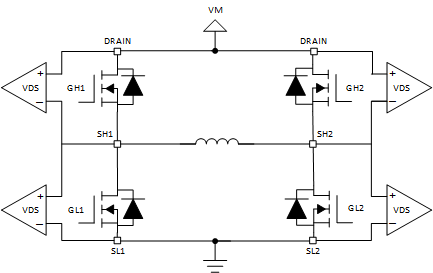
VDS monitors are connected at the drain and source of the FET. The voltage across the drain and source provides information on how much current is running through each FET. As shown in Figure 1, each FET has its own VDS monitor.
 Figure 1. VDS Monitor Schematic
 With TI motor gate drivers, designers can set VDS overcurrent protection threshold values based on the expected current through the FETs and failure conditions they are trying to protect against. This can be done many ways depending on the device used. For example, on DRV8705-Q1 it can be adjusted through VDS_LVL register settings for the SPI interface. For hardware interfaces, designers can set the desired threshold values by connecting resistors to the appropriate pin. Specifications for resistor values and threshold values vary from one device to another and can be found in each device’s datasheet.
In SPI devices, designers also have the option to set the OCP deglitch time. The duration of the overcurrent condition must be greater than the OCP deglitch time for an OCP condition to occur through the VDS register. OCP deglitch time preferences can vary depending on the time it takes to charge the FETs. The longer it takes to charge the FETs, the longer the OCP deglitch time is to ensure the FETs turn on and prevent false OCP conditions. For devices with a hardware interface, the OCP deglitch time falls within a range, specific to each device, which cannot be changed. In the event of an OCP condition, the FETs are disabled to prevent any damage. The specifics of a device’s response and recovery from an OCP condition vary from one to device to another.