SLVAEX3 October 2020 TPS8802 , TPS8804
3.1.1 Photodiode Input Amplifier Model
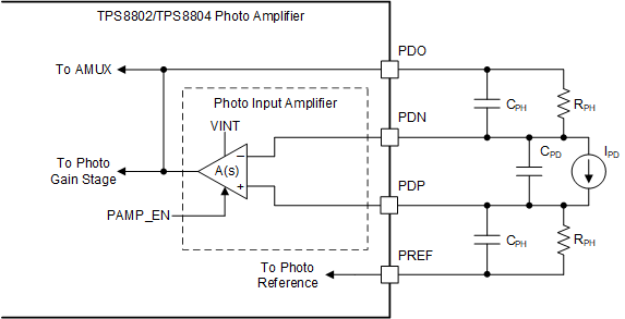
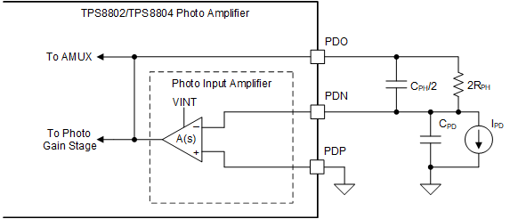
Using a photodiode model consisting of a capacitor and current source, the photo input amplifier system can be modeled as a combination of linear circuit elements shown in Figure 3-1. To simplify the analysis, the PREF photo reference is approximated as a small-signal ground, and the two photo resistors and capacitors are combined in series. The simplified circuit is shown in Figure 3-2. The op-amp is modeled with frequency-dependent open-loop gain A(s). The op-amp open-loop gain is 1 at the gain-bandwidth frequency fGBW.
 Figure 3-1 Photo Input Amplifier
Model
 Figure 3-2 Simplified Photo Input Amplifier
Model
Figure 3-2 Simplified Photo Input Amplifier
ModelEquation 1 shows the open loop transfer function from PDO to PDN. This equation provides insight on how to stabilize the feedback loop. The compensation capacitor CPH must be sized to place the zero frequency below the closed loop unity gain frequency for sufficient phase margin. A phase margin of over 70° prevents overshoot and reduces noise on the output. This is achieved when the zero frequency is less than the unity gain frequency by at least a factor of 3. The zero frequency and unity gain frequency are calculated in Equation 2 and Equation 3. These two equations set a lower limit on the compensation capacitance, shown in Equation 4, using the assumption that CPH is less than CPD. The photo input amplifier has a minimum unity gain bandwidth fGBW of 1 MHz. Set fGBW to 1 MHz when calculating the minimum compensation capacitance.
The compensation capacitance sets the closed loop bandwidth of the amplifier. Solving the closed loop amplifier output PDO in terms of the input current IPD results in Equation 5. The Equation 5 denominator approximately equals 1 at frequencies below the unity gain frequency calculated in Equation 3. In this condition, Equation 5 can be simplified to Equation 6. Equation 6 demonstrates that the photo amplifier output is approximately equal to the photocurrent scaled by the gain resistors and low-pass filtered by the compensation capacitors. Above the unity gain frequency, additional low-pass filtering occurs on the signal.