SLVAEX4A January 2021 – May 2021 TPS272C45
1 Reference Design with TPS272C45
By combining SPI Communication with the existing protection features of TI’s Smart High Side Switches, a designer can have the confidence that their system will be protected while quickly controlling a device’s power rail with the fast data rate associated with SPI. For more information on High side switch protection features such as adjustable current limit and high accuracy current sense, refer to the following app notes on the subjects:
- High Accuracy Current Sense of Smart High Side Switches – SLVAE08
- Adjustable Current Limit of Smart Power Switches – SLVA859
SPI integration is a key care-about in industrial applications. With the emergence of increasingly complex industrial designs and the digitization of manufacturing, industrial applications are becoming more efficient with less waste. To optimize a system through this growth of technology, it is essential for industries to identify where they can improve their processes and leverage new devices and features that support integration of different devices, predictive maintenance, and fast speed.
SPI allows a user to communicate directly with the processor on the back end side of a system thus limiting the need for numerous separate I/O lines. In the case of the TPS272C45, a minimum of three I/O lines are required: EN1, EN2, and FLT. In common industrial applications such as digital I/O modules it is a common requirement to drive up to sixteen individual loads. With each TPS272C45 dual channel device responsible for two loads this would translate to eight TPS272C45 devices and twenty four I/O lines on the microcontroller. Instead of requiring twenty four individually controlled and isolated I/O lines a SPI interface can be used to simplify the design. The system block diagram below in Figure 1-1 uses a single SPI command to trigger sixteen inputs while producing an output signal representing the eight FLTx lines.
 Figure 1-1 Block Diagram for SPI
Expander
Figure 1-1 Block Diagram for SPI
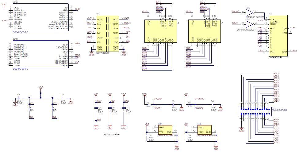
ExpanderIn this system the microcontroller acts as SPI master and writes a 16-bit word into the two SN74HC594-Q1’s shift registers via its SPI peripheral. This in turn updates the sixteen ENx signals of the connected TPS272C45s simultaneously with the rising CS# edge of the SPI signal. Additionally the SPI master microcontroller can read the FLTx data byte of the SN74HC165 that correlates to the eight individual fault lines of the attached TPS272C45s. A schematic of the overall “SPI expander” can be seen below in Figure 1-2.
 Figure 1-2 SPI Expander
Components
Figure 1-2 SPI Expander
ComponentsThe ISO7741 isolator provides high performance quad-channel digital isolation preventing noisy and potentially harmful currents on the device data lines. This device has the advantage of small die space compared to larger optocouplers which require multiple external components. The ISO7741 only requires two external bypass capacitors for a complete design.
The SN74HCS594 8-bit serial-in parallel-out shift register feeds an 8-bit D-type storage register. This register is communicated with the MOSI line of the microcontroller to individually enable and disable the attached EN lines of the TPS272C45. Equipped with Schmitt-Triggered inputs this shift register will eliminate erroneous data outputs due to noisy input signals, and reduces the overall current drawn by the system. The storage and shift register clocks (RCLK and SRCLK) are tied together to cause the shift register to be one count pulse ahead of the storage register. The SN74HC165: 8-bit parallel-in serial-out shift register takes the FLT signals from the connected high-side switches and outputs a serial QH digital signal back to the microcontroller. When SH/LD! Is low, the device loads all the 8 bits simultaneously through the parallel load input and shifts the data when CLK toggles on the rising edge.
It is important to note that while this reference implementation uses the TPS272C45 any Texas Instruments high side switch could use the same design to enable SPI interaction. The ENx and FLTx signals that get relayed in between the shift registers and high side switches are simple digital signals and can be used on devices such as the TPS1H100-Q1, TPS27S100, or any other high side switch from Texas Instruments. It is also important to note that the design described in this application note is a starter reference solution. The design is by no means meant to be comprehensive and many aspect of interfacing with the high side switch are omitted. While sensing load current through the analog sense pin is not supported in this implementation it can easily be added in design via a simple analog power multiplexer.