SLVAEZ2 September 2020 – MONTH TPSM41625
2 Effect of Reducing Output Capacitance on Loop Response
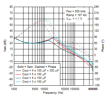
Figure 2-1 shows the measured loop response of the TPSM41625 with different output capacitor configurations. The capacitor configurations span from the initial design shown in Figure 1-1, which is based on the TPSM41625EVM evaluation module and consists of a bulk 330-μF polymer (6TPE330MAA) and four 100-μF ceramic (GRM32EC70J107ME15L) capacitors, down to a design using only three of the same 100-μF ceramic capacitors.
 Figure 2-1 Bode plot for
different Cout (12-V input, 1.8-V output)
Figure 2-1 Bode plot for
different Cout (12-V input, 1.8-V output)For the default evaluation module design, the bulk capacitor contributes an ESR zero which provides phase boost. The phase margin is almost 60° at the loop crossover frequency of 105 kHz where the gain curve crosses 0 dB. The phase curves are lower when the bulk capacitor (and the zero from the ESR) is removed. Decreasing the number of ceramic capacitors pushes the loop crossover frequency higher with decreasing phase margin.
With only 3 x 100 μF of nominal ceramic output capacitance, the loop crossover frequency is 148 kHz with a phase margin of 23° and gain margin of 8 dB. The typical recommendations are to have a minimum of 45° of phase margin and greater than 10 dB of gain margin. Furthermore, while crossover frequencies up to 1/5 of the switching frequency are acceptable for TPSM41625 designs, a crossover frequency of 148 kHz may be considered too high for a switching frequency (Fsw) of 500 kHz. The subsequent sections of this report show different adjustments that can be made to the design to stabilize the control loop for this 3 x 100 μF (300 μF) nominal ceramic output capacitor configuration.