SLVAEZ4 June 2021 TPS272C45
3 Multiplexed Current Limit
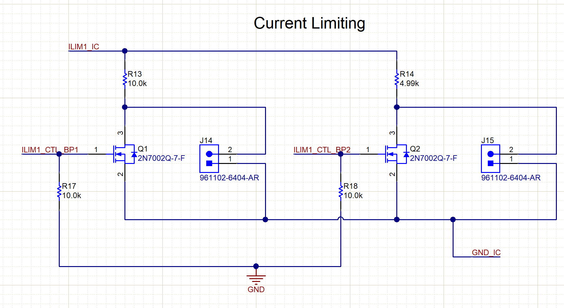
The TPS272C45EVM provides an interface for the microcontroller to pragmatically switch between two or more current limits on an individual ILIM pin. This is accomplished by the use of a MOSFET controlled by the microcontroller’s GPIO pin to switch the resistance value between the ILIM pin and GND. The hardware schematic of this setup is shown in Figure 3-1.
 Figure 3-1 Multiplexed Current Limit
In the tps272c45_multiplexed_current_limit code example the two MOSFETs connected to the ILIM1 pin on the TPS272C45EVM are used to demonstrate how to switch between two separate current limits using software. By default, the MSP430 configures the TPS272C45EVM to use the R13 resistor as the current limit. This is done by using the Q1 MOSFET on the TPS272C45EVM to enable the path from R13 to GND_IC. With the Q1 MOSFET enabled the MSP430 microcontroller drives low the gate of Q2’s MOSFET and effectively shuts off the connection to R14. In this application, S1 turns on and off VOUT1 while S2 switches between R13 and R14 as the configured current limit. VOUT2 is not used in this example.
It is important when using the multiplexed current limit configuration to enable only one resistor on the ILIM pin at a time. The ILIM pin is sensitive to any capacitance so enabling both resistor may lead to unreliable behavior due to the combined trace lengths. The software snippet used to enable R13 and disable R14 are shown here:
#pragma vector=PORT1_VECTOR
__interrupt void Port_1(void)
{
    switch (__even_in_range(P1IV, 16))
    {
        case P1IV_NONE:
            break;   // Vector  0: no interrupt
        case P1IV_P1IFG0:
            break;   // Vector  2: P1.0
        case P1IV_P1IFG1:
            ILIM1_OUT ^= ILIM1_PIN;
            ILIM2_OUT ^= ILIM2_PIN;
            P1OUT ^= BIT0;
            P4OUT ^= BIT7;
            break;
        case P1IV_P1IFG2:
            break;   // Vector  6: P1.2
        case P1IV_P1IFG3:
            break;   // Vector  8: P1.3
        case P1IV_P1IFG4:
            break;
        case P1IV_P1IFG5:
            break;   // Vector 12: P1.5
        case P1IV_P1IFG6:
            break;   // Vector 14: P1.6
        case P1IV_P1IFG7:
            break;   // Vector 16: P1.7
        default:
            break;
    }
}
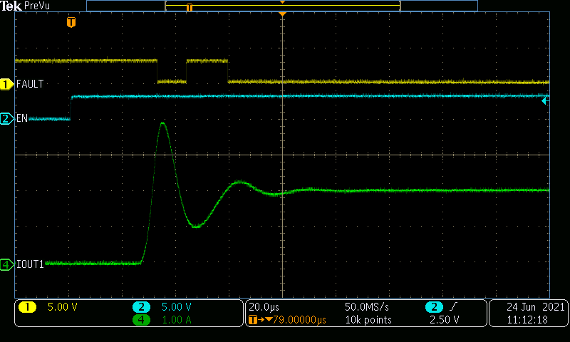
The current limit engaging on the R13 resistance of 10kΩ (2A nominal current limit) can be seen below in Figure 3-2
 Figure 3-2 Current Limit - Permanent Short
2A
Figure 3-2 Current Limit - Permanent Short
2ANote that in the waveform below that when the current limit engages the FAULT pin initially goes low, briefly goes high, and then remains low for the duration of the overcurrent event. The initial low state of the FAULT and brief high state is due to the current limit engaging and temporarily dropping the current to below the set current limit value. To prevent any race condition in software for handling the FAULT pin, the pin interrupt should trigger a timer that acts as a deglitch filter. This is implemented in the tps272c45_adc_polling code example and the code block of the timer ISR that implements the deglitch filter is shown here:
// Timer0 A0 interrupt service routine
#pragma vector=TIMER0_A0_VECTOR
__interrupt void TIMER0_A0_ISR(void)
{
    /* If the fault is gone, return to normal operation */
    if(FAULT_IN | FAULT_PIN)
    {
        TA0CTL = 0;

        if(en1On == true)
        {
            P1OUT |= BIT0;
        }
        else
        {
            P1OUT &= ~BIT0;
        }

        if (en2On == true)
        {
            P4OUT |= BIT7;
        }
        else
        {
            P4OUT &= ~BIT7;
        }
    }
}