SLVAF44 April 2021 TPS5432
3 Unexpected Protection Behavior During the Load Release of SoC Chipset
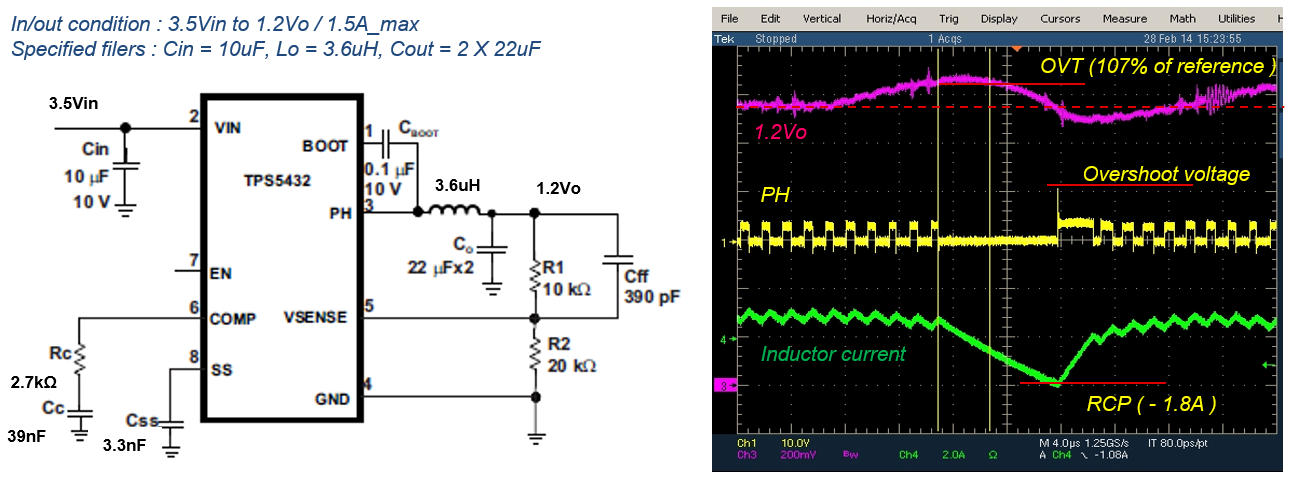
Figure 3-1 (left) shows the TPS5432 application to generate 1.2Vo rail for SoC core voltage in the TV application. The problem is that there is an excessive overshoot voltage on PH node as shown in Figure 3-1 (right). As the root cause of the overshoot voltage, Vout (VSENSE pin voltage) is greater than the OVTP threshold during the load release of SoC chipset, the high side MOSFET is disabled preventing current from flowing to the output and minimizing output overshoot. However, the converter sinks current through its low side FET.
As an additional RCP (Reverse current protection) scheme, the control circuit turns off the low side MOSFET when the reverse current is more than 1.8 A. At this time, Current starts flowing though on the body diode of high side FET to input capacitor. When Vout drops lower than the OVTP threshold, high side MOSFET is allowed to turn on the next clock cycle. Then it causes a severe ring voltage because of an accumulated charge into input capacitor, the leakage inductance on PCB layout and capacitance of FETs.
 Figure 3-1 An Unexpected Protection
Behavior During the Load Release of SoC chipset
Figure 3-1 An Unexpected Protection
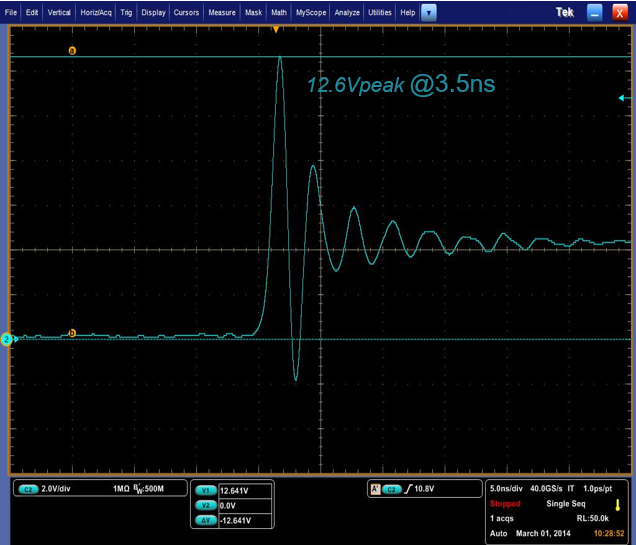
Behavior During the Load Release of SoC chipsetThe worst overshoot voltage reaches to 12.6 V peak for 3.5ns in this application as shown in Figure 3-2. To figure out the worst case, a high-resolution Oscilloscope (Tektronix DPO7354C model with 500MHz Bandwidth) and Probe (P6139B probe) are used. Even though this overshoot voltage will not cause immediate device damage, it can affect a long-term device reliability.
 Figure 3-2 The Worst Overshoot Voltage in
the Application