SLVAF52B July   2021  – November 2021 AFE8092 , TPS62913


  1.   Trademarks
  2. 1Introduction
  3. 2System Description
    1. 2.1 AFE80xx Noise and Ripple Requirements
    2. 2.2 AFE80xx Supply Settling and EVM for TDD Operations
    3. 2.3 Block Diagram
      1. 2.3.1 Proposed Power Architecture
      2. 2.3.2 Power Sequencing
    4. 2.4 Power Supply Design Consideration
  4. 3Tests and Results
    1. 3.1 Test Methodology
      1. 3.1.1 Phase Noise (Transmit) (dBc/Hz)
      2. 3.1.2 EVM for Frequency Division Multiplexing (FDD) Mode(%)
      3. 3.1.3 EVM for TDD Mode(%)
      4. 3.1.4 Receive (RX) Spectrum (Power Supply Spurious)
      5. 3.1.5 Power Efficiency
    2. 3.2 Test Conditions
    3. 3.3 Test Results
      1. 3.3.1 Phase Noise
      2. 3.3.2 EVM for FDD Mode
      3. 3.3.3 EVM for TDD Mode
      4. 3.3.4 RX Spectrum
      5. 3.3.5 Power Efficiency
  5. 4Conclusion
  6. 5References
  7. 6Revision History

EVM for FDD Mode

For EVM plot in FDD mode, all transmit and receive pairs are configured for 20-MHz 5G NR Spectrum set at 3.5 GHz. EVM waveform in Figure 3-2 indicates 0.33% average constellation deviation across symbols and first symbol peak deviation close to 1% which is well below the target of 2%. CH1 spectrum also represent in band spurious free spectrum for occupied bandwidth.
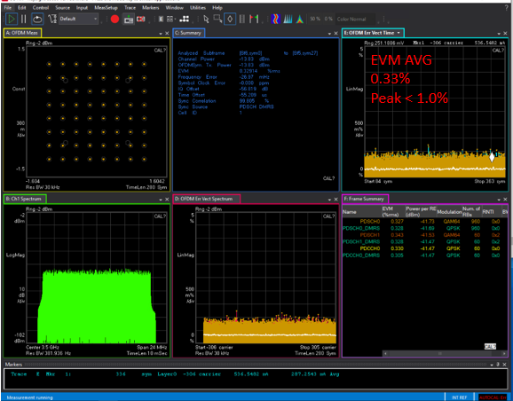
GUID-20210614-CA0I-QZD9-M73N-KRXFXRLZN2TS-low.png Figure 3-2 EVM for FDD Mode (5G NR Spectrum)