SLVAF52B July 2021 – November 2021 AFE8092 , TPS62913
3.3.3 EVM for TDD Mode
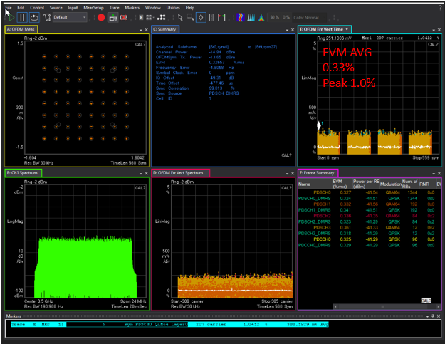
For EVM plot in TDD mode all transmit and receive pairs are configured for 20-MHz 5G NR Spectrum set at 3.5 GHz. 75% Receive and 25% Transmit duty period of 100-Hz periodic pulse is generated using FPGA capture card and configured to toggle AFE8092 CPLD pins IO_DIFFIO-L4P and IO_DIFFIO-L4N.
EVM waveform in Figure 3-3 indicates 0.33% average constellation deviation across symbols and first symbol peak deviation close to 1% which is well below target of below 2%. CH1 spectrum also represent in band spurious free spectrum for occupied channel bandwidth.
 Figure 3-3 EVM for TDD Mode (5G NR
Spectrum)
Figure 3-3 EVM for TDD Mode (5G NR
Spectrum)In complete system applications with external PA, the RX to TX guard time can be adjusted such that the power supply is settled before data is transmitted on output channel.