SLVAF55 July 2021 TPS62130 , TPS62901 , TPS62902 , TPS62903
3.1 Smaller Package and Fewer External Components
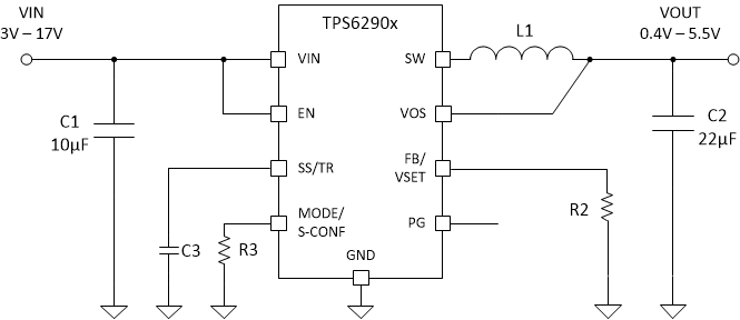
The QFN package of TPS6290x is one third the size of the previous generation, however the size of the package is not the only thing that has shrunk. The total solution size is reduced by more than 30% as well. To achieve both of these reductions, TPS6290x has decreased the number of pins on the package from 16 to 9, allowing the package to shrink and decreasing the passives needed to configure the device. The result saves precious board space, BOM costs and design time.
 Figure 3-1 Typical
application schematic of the TPS621x0
 Figure 3-2 Typical
application schematic of the TPS6290x