SLVAF68 July 2021 TPS61086
2 Proposed Circuit for Negative-to-Negative Boost Application
In non-isolated DC-to-DC applications, there are two input rails connecting to the DC source and two output rails connecting to the load. One rail is always shared between the input and the output, and this common rail is designated the system ground which is the ground for the power stage. The ground of the TPS61086 may not always be connected to the system ground if the TPS61086 is being used in a way other than its primary intended application.
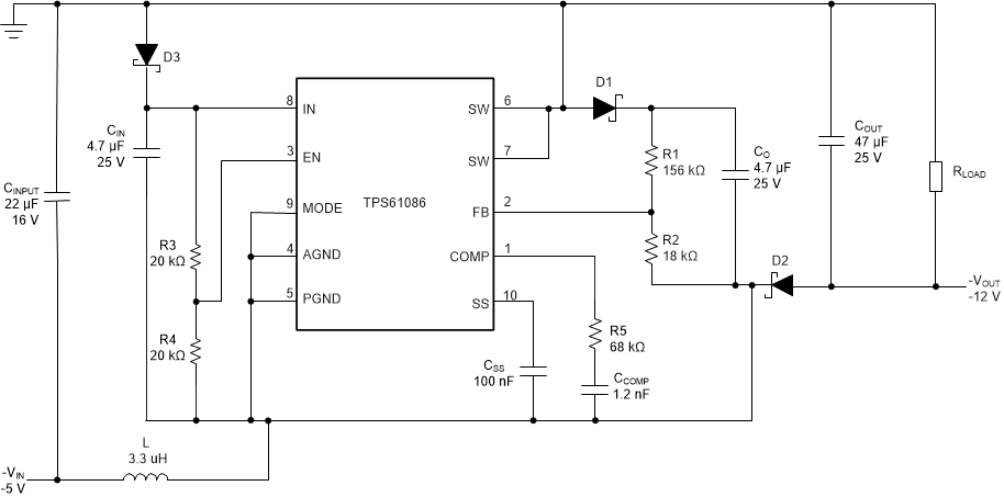
Figure 2-1 shows the proposed circuit for negative-to-negative boost application, and the ground of TPS61086 is not connected directly to the system ground. In this case, the sensing point for the feedback is not direct from the actual load since the feedback voltage always needs to be referenced to the ground of the TPS61086.
 Figure 2-1 Negative-to-Negative Boost
Converter
Figure 2-1 Negative-to-Negative Boost
ConverterThe regulator loop can be compensated by adjusting R5 and Ccomp connected to COMP pin which is the output of the internal transconductance error amplifier.
This conversion belongs to the family
of indirect energy transfer converters, and the power process involves an
energy-storing phase and energy-release phase. During the on time, the inductor
stores energy, and the output capacitor alone powers the load. When the internal
power switch of the TPS61086 closes, VIN immediately appears across the
main inductor (L), and the inductor current reaches a peak value as it is defined
by
Equation 1.
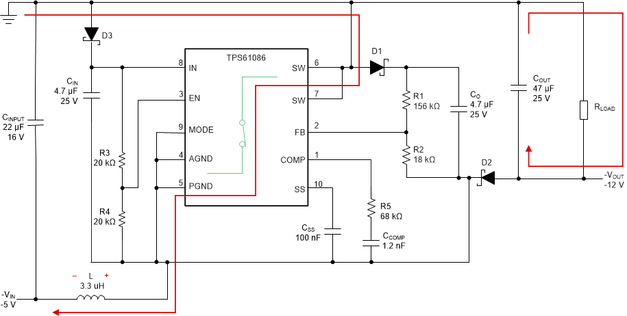
Ia represents the condition for t=0. In the case of the discontinuous conduction mode case, it can be zero, or a certain value for continuous conduction mode operation. Figure 2-2 shows the situation where the load and the output capacitor are left alone while the power switch closes, and the output capacitor voltage will decrease during this on time.
 Figure 2-2 The Internal Power Switch of
the TPS61086 is On
Figure 2-2 The Internal Power Switch of
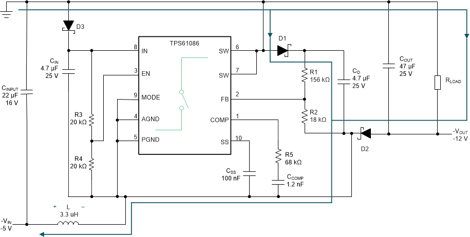
the TPS61086 is OnFigure 2-3 shows the status when the internal power switch of the TPS61086 turns off, and the inductor current must find a circulating path in this case. At the power switch opening, the stored inductor energy appears in series with the input source (VIN) and contributes to supply the output. Also, the inductor voltage reverses trying to keep the ampere-turns constant, and this voltage comes in series the input voltage.
During the off time, the energy stored
in the inductor during the on time depletes to a rate described by
Equation 2.
The diode (D1) routes the inductor current to the capacitor (CO) for the feedback path to regulate the output voltage (VOUT) since the feedback voltage always needs to be referenced to the ground of the TPS61086. Also, the diode (D2) routes the inductor current to the capacitor (COUT) and the output load (RLOAD), and this will help dump the stored inductor energy into COUT and RLOAD. When the new cycle occurs, the internal power switch of the TPS61086 closes again as shown in Figure 2-2.
 Figure 2-3 The Internal Power Switch of
The TPS61086 is Off