SLVAF68 July 2021 TPS61086
3 Simulation and Experimental Results
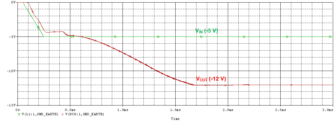
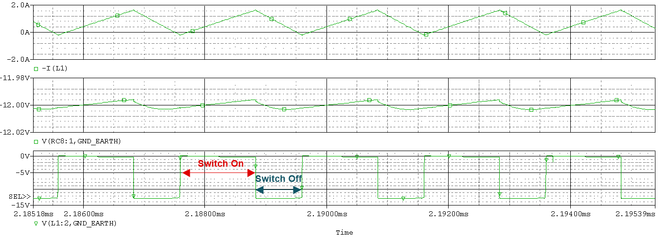
To verify the operation and performance of the proposed application method, the critical waveforms including the output voltage and the inductor current are measured as shown in the figures from Figure 3-1 to Figure 3-3. The results shown in Figure 3-1 and Figure 3-2 have been obtained by PSpice simulation, and it can be seen that the TPS61086 operates properly for negative-to-negative boost applications.
Figure 3-1 shows -12 V output voltage in red starting up with -5 V input voltage in green.
 Figure 3-1 PSpice Simulation Result at
Startup
Figure 3-1 PSpice Simulation Result at
StartupFigure 3-2 shows the inductor current, the output voltage and the switching node of the inductor at steady state activating the internal power switch on and off, and the output current is 200mA. As shown in Figure 3-2, when the internal power switch is on, the switching node of the inductor goes up to the system ground. On the opposite, when the internal power switch is off, this will help dump the stored inductor energy into COUT and RLOAD.
 Figure 3-2 PSpice Simulation Result at
Steady State
Figure 3-2 PSpice Simulation Result at
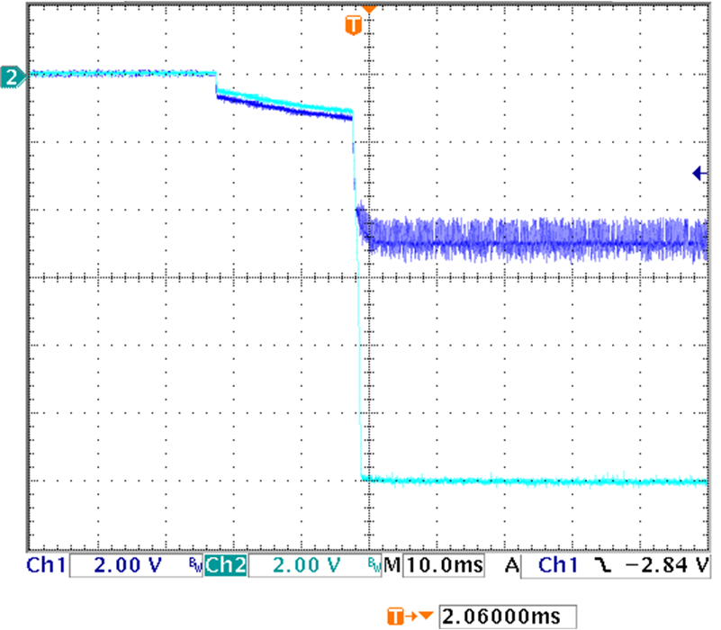
Steady StateFigure 3-3 shows an experimental result to create -12 V output (Ch2 in light blue, 2 V/div) from -5 V input (Ch1 in blue, 2 V/div). As shown in Figure 3-3, the test waveform matches the simulation result well, and the actual input voltage range is from -2.9 to -6 V for the proper regulation on the output (-12 V).
 Figure 3-3 Test Waveform from -5 V Input
to -12 V Output
Figure 3-3 Test Waveform from -5 V Input
to -12 V OutputIt is important to note that this kind of new configurations might have different voltage levels on each pin of the TPS61086 compared to its primary intended application, and the desired operation can be successfully achieved by complete understanding on the both the internal construction of the TPS61086 and the power stage topologies.