SLVAF74 July 2021 TPS2372 , TPS2373 , TPS23730 , TPS23731 , TPS23734 , TPS2375 , TPS2375-1 , TPS23750 , TPS23751 , TPS23752 , TPS23753A , TPS23754 , TPS23754-1 , TPS23755 , TPS23756 , TPS23757 , TPS23758 , TPS2376 , TPS2376-H , TPS2377 , TPS2377-1 , TPS23770 , TPS2378 , TPS2379
3.1 Schematic Areas
The first area is the PoE Input, see Figure 3-1. This includes the RJ45, the Ethernet PHY (which separates the data and power), the Bob Smith terminations, the rectifier, the EMI filtering components, and the TVS diode. The rectifier can be discrete components or integrated solutions.
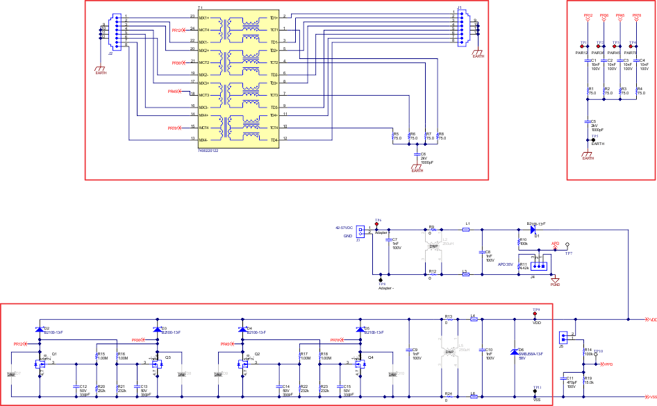 Figure 3-1 PoE Input Section
Figure 3-2 shows the second area, the PoE Settings. These are the components that set or enable different PoE functions. For example, the detection resistor, enabling Auto-MPS, the detection capacitance, and so on. Note that many of these components reference VSS instead of RTN.
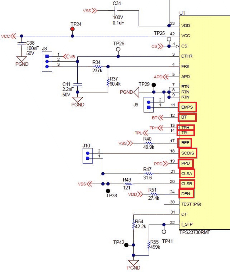 Figure 3-2 PoE IC Settings
In a standalone PD, like the TPS2373, these are the pins and components that are not being sent downstream to a PWM controller.
The next section is the primary side of the DC/DC. This section includes a few subsections: input filter, IC settings, VCC input, primary side feedback components, the primary MOSFETs (and accompanying components), and the primary side of the transformer.
The input filter, illustrated in Figure 3-3, includes the input bulk capacitor, an inductor, and some smaller capacitors. The bulk capacitor must have some ESR to operate, so they are typically electrolytic or aluminum capacitors. These are a good reference point on the board since they are typically easier to see with the naked eye, and they give access to VDD and RTN with large solder pads. The other components of the input filter help reduce input ripple (and thus output ripple).
 Figure 3-3 Input Filter
The PWM IC settings are the rest of the resistors and capacitors on the IC. They set characteristics of the PWM controller. For example, the FRS resistor sets the switching frequency, DT sets the dead time between the two gates (if applicable), and so on. Not shown here is the LINUV input. The LINUV input sets the turn-on and turn-off DC/DC input voltage of the IC.
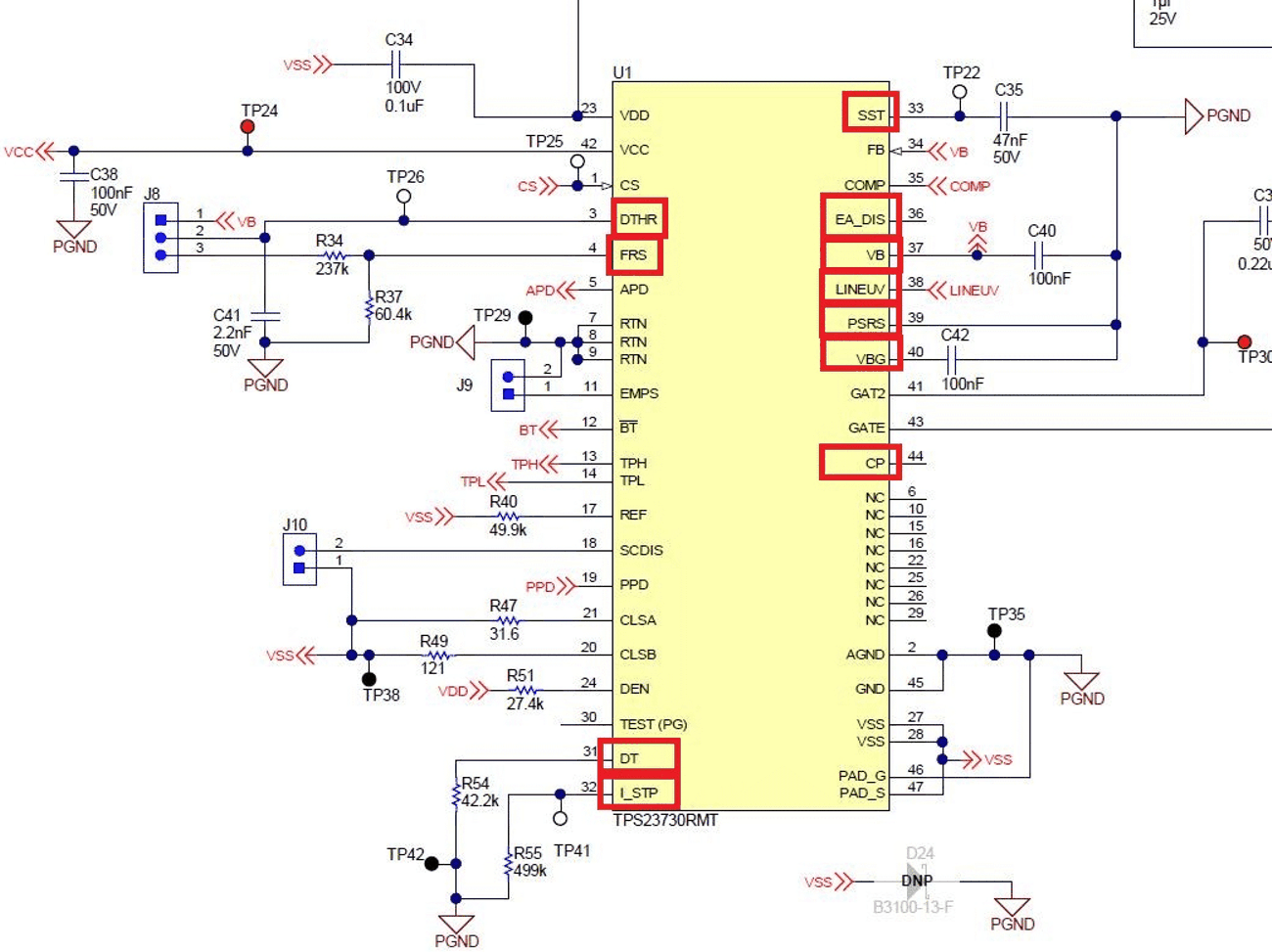 Figure 3-4 DC/DC Pin Settings
The VCC input looks different for different topologies. As previously discussed, VCC is the input power for the IC. In an active clamp forward, the VCC line is taken off the auxiliary winding of the transformer, rectified by two diodes and the ripple is filtered with an inductor. VCC requires a capacitor to store energy for the IC. VCC also requires a smaller bypass capacitor, as does VB and VDD.
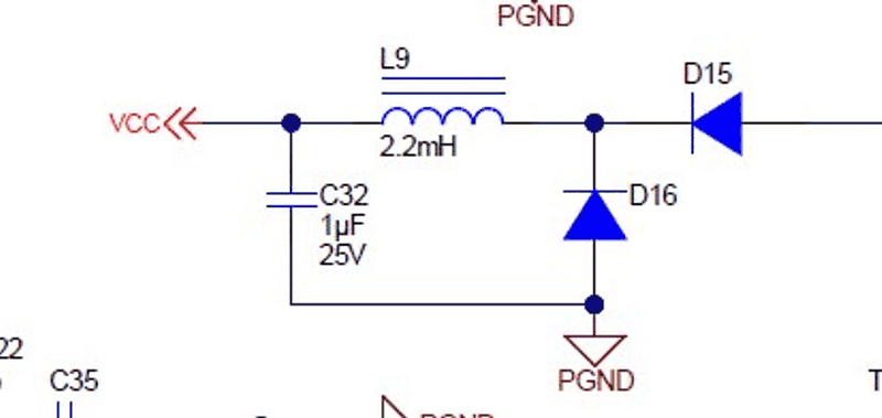 Figure 3-5 VCC Input Circuit for Active
Clamp Forward
Figure 3-5 VCC Input Circuit for Active
Clamp ForwardThe VCC input in a flyback appears similar because it is taken off the auxiliary winding of the transformer. Note that flybacks typically only need a single diode to limit the VCC input current from the auxiliary winding and the resistor to help filter. The VCC capacitor is also required. For primary-side regulation flybacks, additional components appear on the winding that is discussed later.
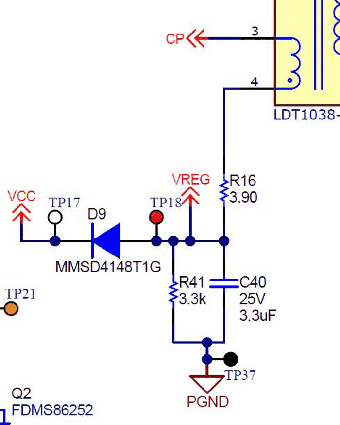 Figure 3-6 VCC Input Circuit for
Primary-Side Regulation Flyback
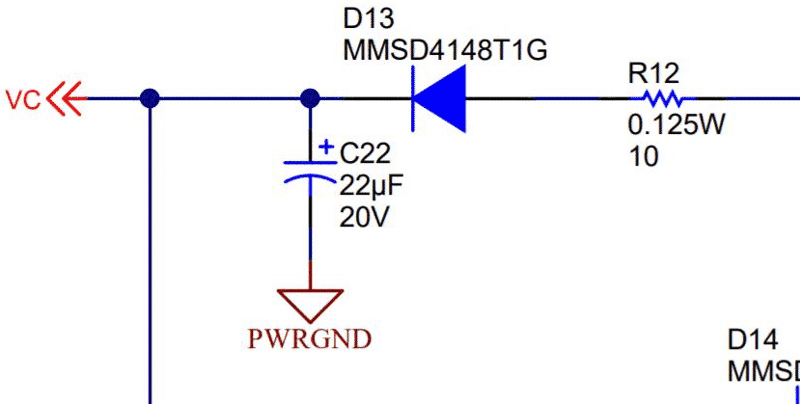 Figure 3-7 VCC Input Circuit for
Optocoupler Flyback
Figure 3-7 VCC Input Circuit for
Optocoupler FlybackBoth PSR and optocoupler feedback designs have components that contribute to the feedback loop on the primary side. PSR designs have the entire feedback network on the primary side.
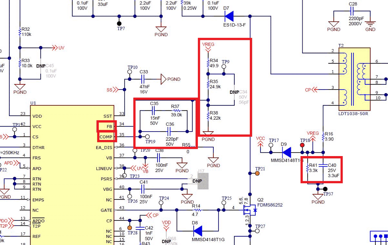 Figure 3-8 Primary Side Feedback PSR
Flyback
Figure 3-8 Primary Side Feedback PSR
FlybackOptocoupler feedback components have their primary side loop components at the optocoupler. Note this is true for both ACF and flyback designs.
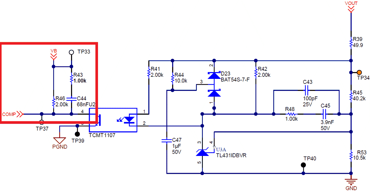 Figure 3-9 Primary Side Feedback
Optocoupler Flyback
Figure 3-9 Primary Side Feedback
Optocoupler FlybackThe next portion of the primary side of the DC/DC is the primary side MOSFETs and accompanying components. For a flyback, there is only one primary MOSFET. This MOSFET requires a gate drive. Sometimes a more robust gate drive, which includes a BJT, is required to turn the MOSFET off faster. All MOSFETs require a DRC clamp. This limits the overshoot voltage so that the MOSFET is not damaged. There is always overshoot because of the primary inductor of the transformer. The current sense or CS resistor, helps set the output current limit.
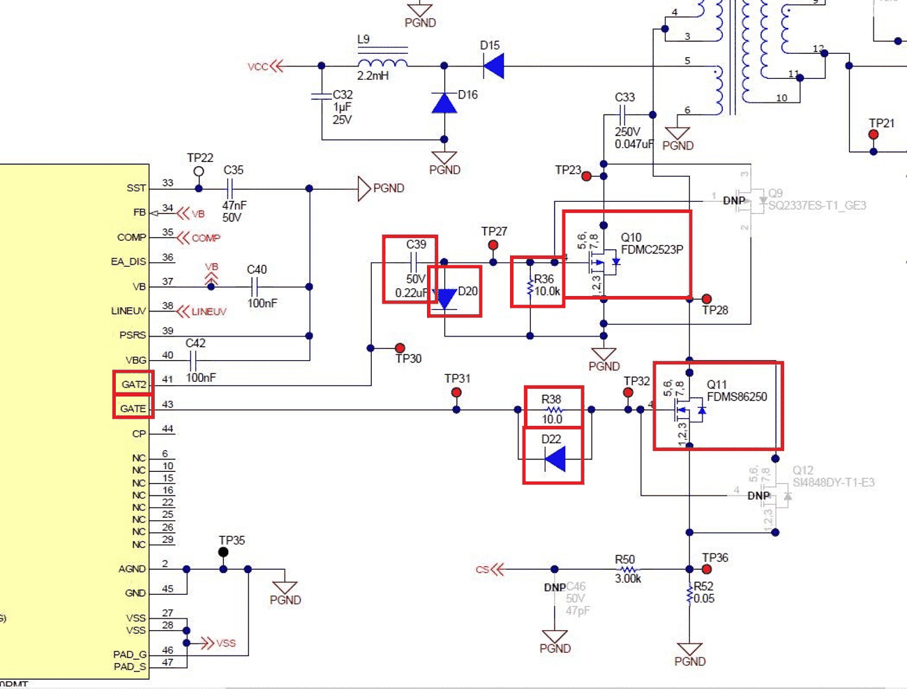 Figure 3-10 Primary Side MOSFETs and
Accompanying Components (Flyback)
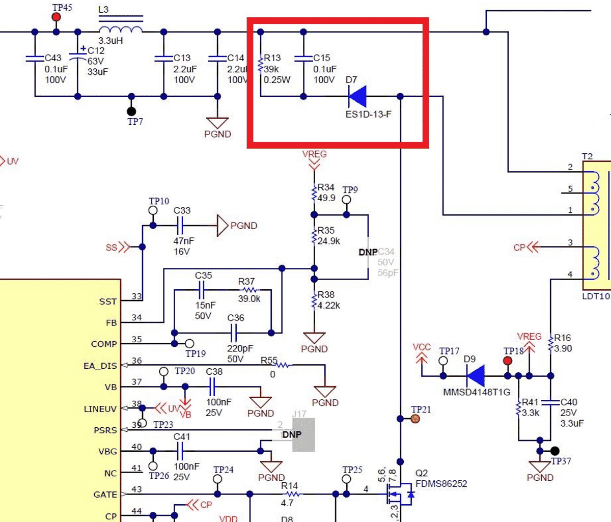 Figure 3-11 Primary Side MOSFET RCD
Snubber
Figure 3-11 Primary Side MOSFET RCD
SnubberAn ACF has two MOSFETs on the primary side. The P-FET provides the active clamp. Both MOSFETs need their respective gate drives. Additionally, the high voltage clamp capacitor is required, but note there is no DRC clamp
Note that MOSFETs in any topology can also have an RC snubber. RC snubbers are placed across the drain to source, and can help reduce the overshoot across the FET. These are not pictured here, but sometimes are useful for overshoot or EMI issues.
Lastly, the primary side has the primary side of the transformer, which includes the primary inductor and the auxiliary winding.
The next section examines the secondary side. This is where the topologies differentiate from one another the most. Diode flybacks are considered the easiest because they have the fewest parts.
Diode flybacks consist of the output diode and accompanying snubber (typically RC).
 Figure 3-12 Secondary Side Diode Rectified
Flyback
Figure 3-12 Secondary Side Diode Rectified
FlybackA synchronous flyback is similar, except that it has a MOSFET instead of a diode. That MOSFET requires a gate drive. The gate drive can be self-driven, as in the transformer drives it, or it can be driven with a pulse transformer or a synchronous rectifier IC. Figure 3-13 through Figure 3-15 provide samples of gate drives and MOSFETs:
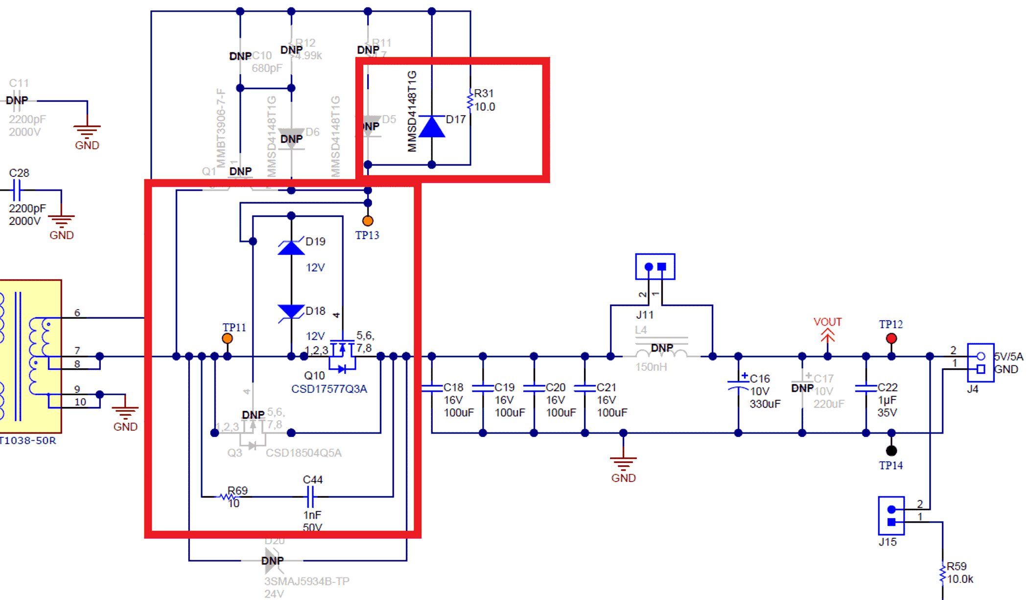 Figure 3-13 Secondary Side Self Driven
Synchronous Flyback A
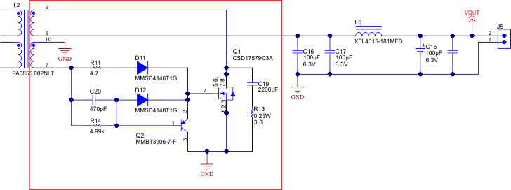 Figure 3-14 Secondary Side Self Driven
Synchronous Flyback B
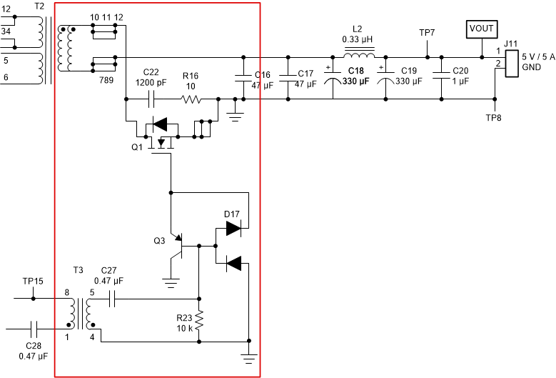 Figure 3-15 Secondary Side Driven
Synchronous Flyback
Figure 3-15 Secondary Side Driven
Synchronous FlybackActive clamp forwards are the most complex topology since they have the most parts and most considerations. Active clamp forwards consist of two MOSFETs, their accompanying gate drives, snubbers (both RC and RCD), and an inductor. Using Figure 3-16, the switching MOSFETs and gate drives are in the dotted-line boxes, and the accompanying RC snubber and RCD clamp are in the solid-line boxes. The green line is considered the parallel MOSFET because the VDS is in parallel with Vout. The red box is considered the series MOSFET because the VDS is in series with the power path. Note, the inductor is optional in flybacks but is required in ACFs.
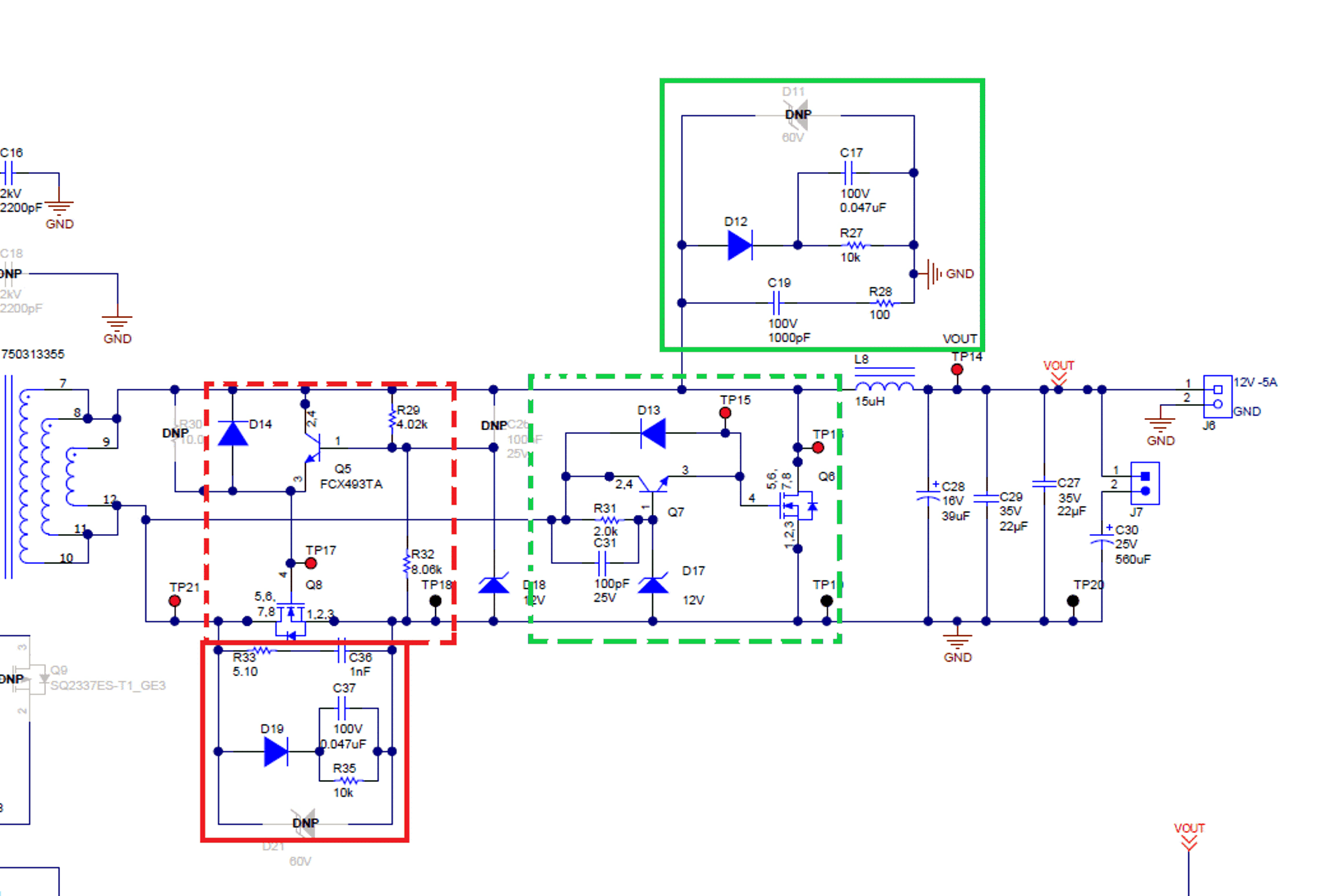 Figure 3-16 Secondary Side Active Clamp
Forward
Figure 3-16 Secondary Side Active Clamp
ForwardAll topologies will have output capacitance. This is usually a mix of electrolytic, aluminum, tantalum polymer and ceramics. Additionally, there may be an inductor to create a PI filter.
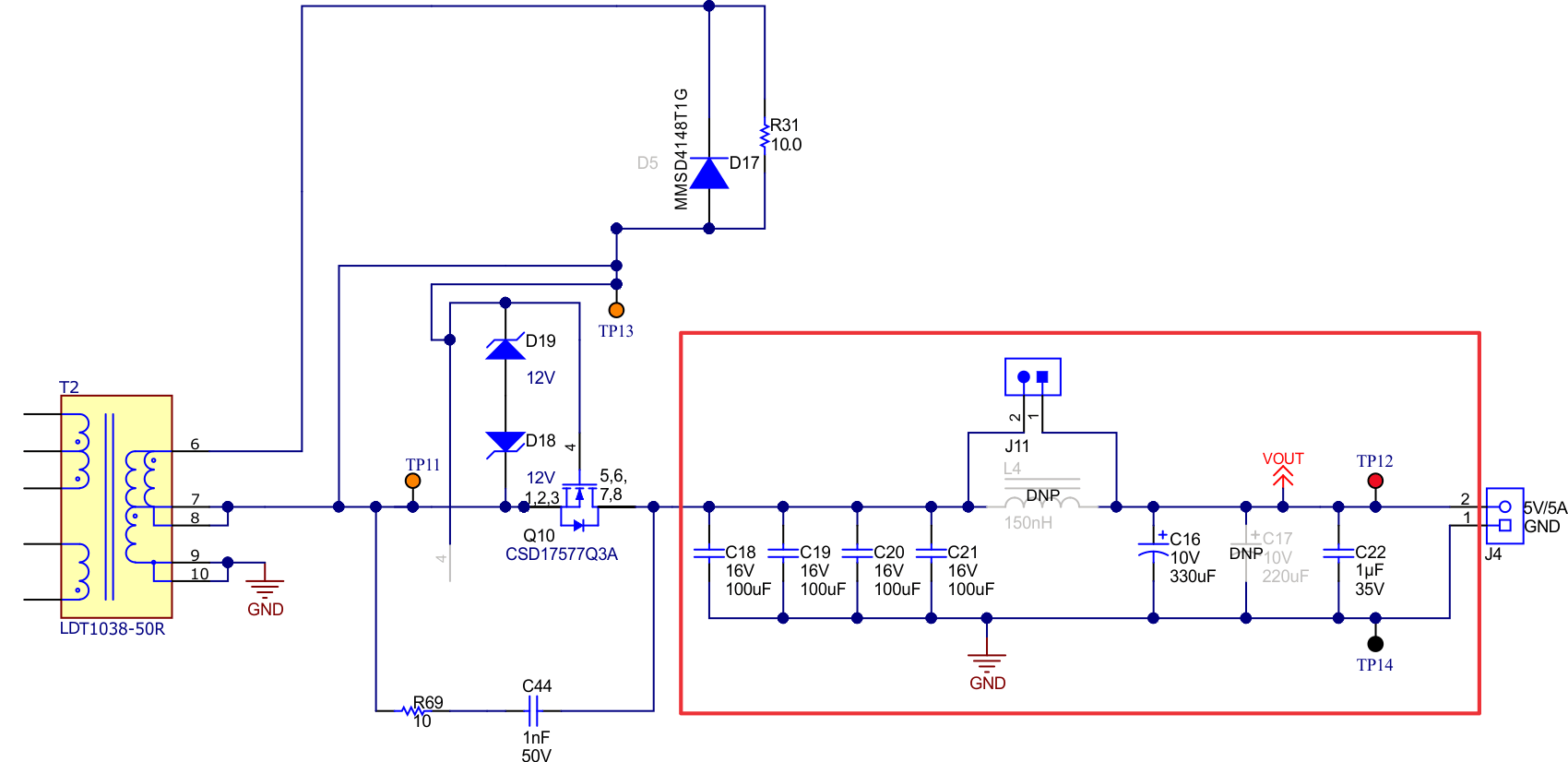 Figure 3-17 Output Capacitance
Finally, the last section is the feedback section, particularly with an optocoupler feedback network, see Figure 3-18. Taken off the output voltage, a TVL, group of resistors and capacitors, and a diode feed into the diode of the optocoupler. These form the poles and zeroes in the loop response, as well as a secondary soft start circuit.
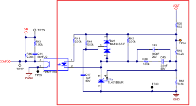 Figure 3-18 Secondary Side Optocoupler
Feedback Network