SLVAFE7 September   2022 LM51551


  1.   Abstract
  2.   Trademarks
  3. 1Introduction
    1. 1.1 Design Specification and Key Challenges
  4. 2High-Voltage Power Supply Design Using SEPIC
    1. 2.1 TI HV Supply Architecture Using SEPIC Topology
    2. 2.2 Switching Frequency Shift
    3. 2.3 Voltage Control by External Signal
  5. 3Test Result
    1. 3.1 Efficiency and Power Consumption (100 kHz vs 250 kHz)
    2. 3.2 Linearity of Output Voltages vs VBIAS
    3. 3.3 Output Ripple Measurement
    4. 3.4 Load Transient Test
    5. 3.5 Overload Protection
    6. 3.6 Thermal Image
  6. 4Summary
  7. 5References

Overload Protection

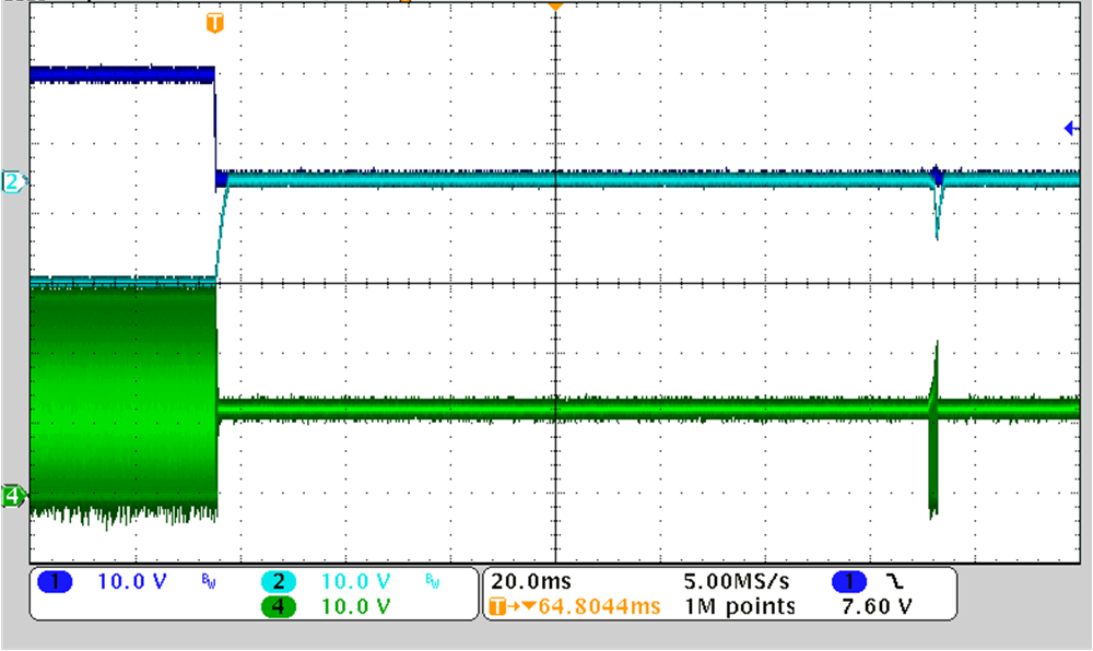
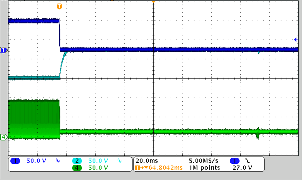
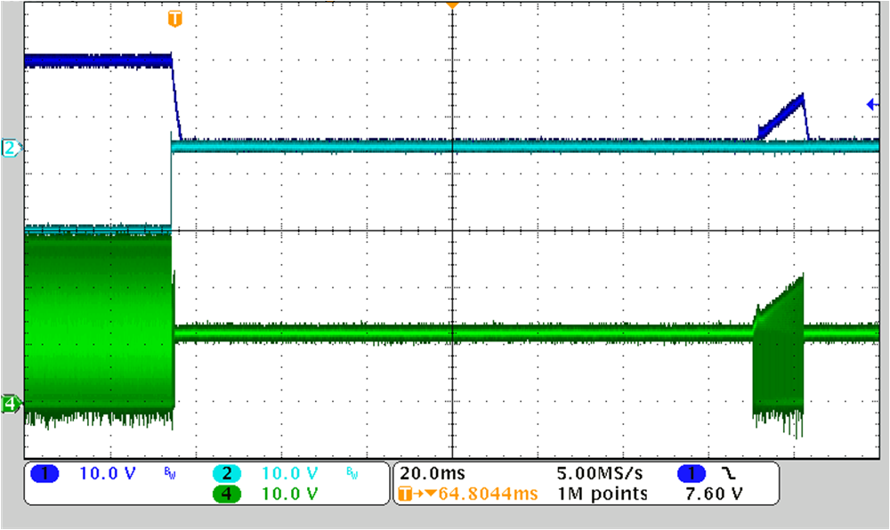
Figure 3-11 through Figure 3-14 show the output overload protection when one of the outputs goes overload.
GUID-20220808-SS0I-Q4MB-KWKV-XGWLBZDPGZPL-low.png
CH1: VOUT1, CH2: VOUT2, CH4: VSW
Figure 3-11 12-V Input, ±15 V, 10 mA, Output1 Overload
GUID-20220808-SS0I-L61J-7GPW-VTFBB3MRG4F8-low.png
CH1: VOUT1, CH2: VOUT2, CH3: IOUT2, CH4: VSW
Figure 3-13 12-V Input, ±75 V, 10 mA, Output1 Overload
GUID-20220808-SS0I-N0WQ-PC3M-BXJXS1J5W6PR-low.png
CH1: VOUT1, CH2: VOUT2, CH4: VSW
Figure 3-12 12-V Input, ±75 V, 10 mA, Output2 Overload
GUID-20220808-SS0I-XLFL-ZQLB-7W6CKN6QS3JH-low.png
CH1: VOUT1, CH2: VOUT2, CH3: IOUT2, CH4: VSW
Figure 3-14 12-V Input, ±75 V, 10 mA, Output2 Overload