SLVAFE7 September   2022 LM51551


  1.   Abstract
  2.   Trademarks
  3. 1Introduction
    1. 1.1 Design Specification and Key Challenges
  4. 2High-Voltage Power Supply Design Using SEPIC
    1. 2.1 TI HV Supply Architecture Using SEPIC Topology
    2. 2.2 Switching Frequency Shift
    3. 2.3 Voltage Control by External Signal
  5. 3Test Result
    1. 3.1 Efficiency and Power Consumption (100 kHz vs 250 kHz)
    2. 3.2 Linearity of Output Voltages vs VBIAS
    3. 3.3 Output Ripple Measurement
    4. 3.4 Load Transient Test
    5. 3.5 Overload Protection
    6. 3.6 Thermal Image
  6. 4Summary
  7. 5References

Load Transient Test

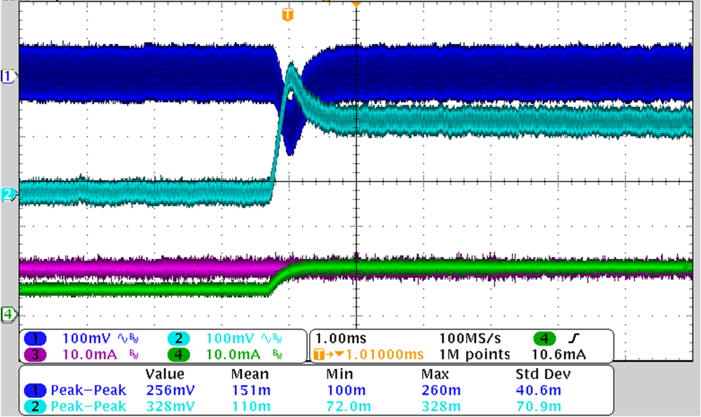
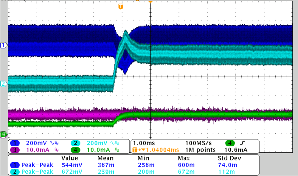
Figure 3-9 and Figure 3-10 show the waveforms of output AC ripples at load transient. The high current level is full load for 10 ms; the low current level is half load for 10 ms, with a slew rate of 0.1 A/μs. As the load on the positive output remains stable, the load on the negative increases from 5 mA to 10 mA, the voltage drops are 151 mV and 367 mV with the output 15 V and 75 V, respectively.
GUID-20220808-SS0I-KJSQ-RBSH-SKLNGJ4GRFJG-low.png
CH1: VOUT1, CH2: VOUT2, CH3: IOUT1, CH4: –IOUT2
Figure 3-9 12-V Input, 15 V, 10 mA, –15 V, 5 mA to 10 mA
GUID-20220808-SS0I-VXWH-DHLZ-L8X1S8CXKNLS-low.png
CH1: VOUT1, CH2: VOUT2, CH3: IOUT1, CH4: –IOUT2
Figure 3-10 12-V Input, 75 V, 10 mA, –75 V, 5 mA to 10 mA