SLVAFG5 November 2022 TPS929240-Q1
2.2 Layout Design
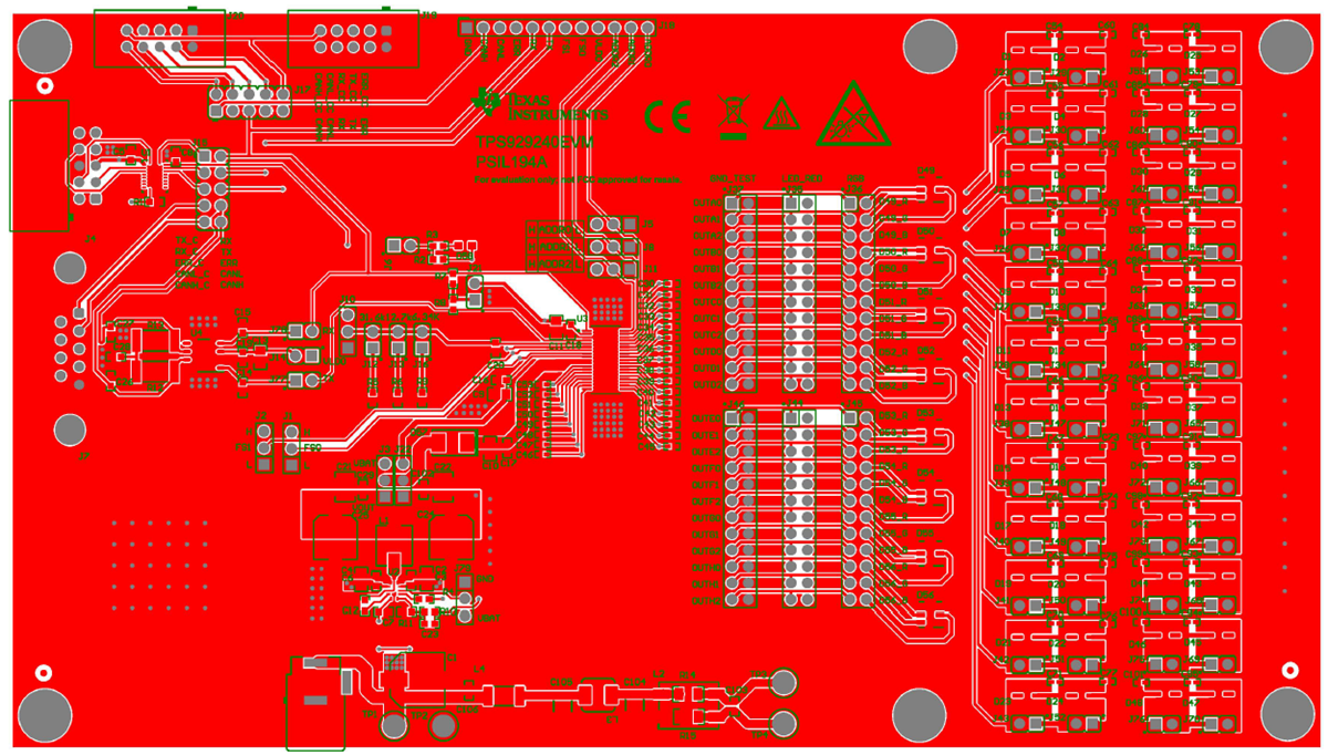
Figure 2-2 shows the layout of TPS929240-Q1 EVM.
- Design large thermal dissipation area connected to thermal pads with multiple thermal vias.
- Place the capacitors (C9, C16, C10, C17, C11, C18) for VBAT, SUPPLY input and VLDO output as close as possible to the pins.
- The RREF resistor needs to be placed as close as possible to the REF pin.
- Make sure the 1 nF capacitors on each output channels are close to the IC.
- The jumpers J1 to J76 are removed during the test to avoid the unexpected radiated noise coupling during the bulk current injection. The jumpers in the EVM are only for evaluation convenience, which normally are not required in a real application.
 Figure 2-2 TPS929240-Q1 EVM Layout
Illustration for BCI Test