SLVK099B March 2022 – September 2023 TPS7H5001-SP , TPS7H5002-SP , TPS7H5003-SP , TPS7H5004-SP
PRODUCTION DATA
- 1
- Abstract
- Trademarks
- 1 Introduction
- 2 Single-Event Effects (SEE)
- 3 Device and Test Board Information
- 4 Irradiation Facility and Setup
- 5 Depth, Range, and LETEFF Calculation
- 6 Test Setup and Procedures
- 7 Destructive Single-Event Effects (DSEE)
- 8 Single-Event Transients (SET)
- 9 Event Rate Calculations
- 10Summary
- A Total Ionizing Dose from SEE Experiments
- B References
- C Revision History
3 Device and Test Board Information
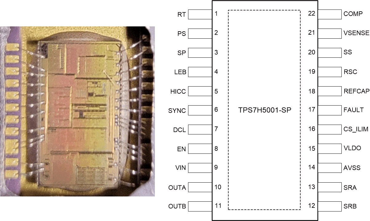
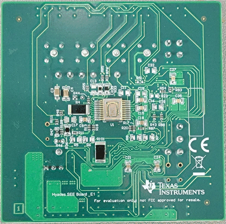
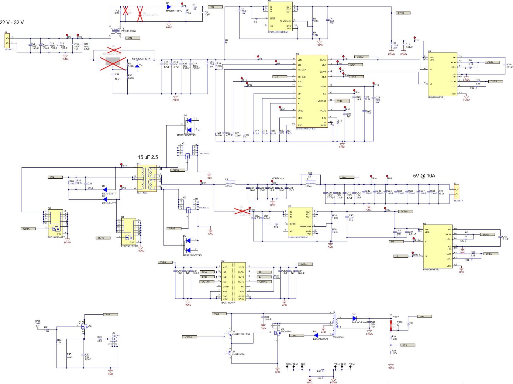
The TPS7H500x-SP is packaged in a 22-pin thermally-enhanced ceramic flatpack package as shown in Figure 3-1. To see specific pinout differences between TPS7H5001/2/3/4-SP, see the TPS7H5001-SP product page. A special test board designed specifically for radiation testing was used to evaluate the performance of the TPS7H500x-SP under heavy-ions. The test board is shown in Figure 3-2. Figure 3-3 shows the board schematics.
The package was delidded to reveal the die face for all heavy-ion testing.
 Figure 3-1 Photograph of Delidded
TPS7H500x-SP (Left) and Pinout Diagram (Right)
 Figure 3-2 TPS7H500x-SP SEE Test Board
Top View
Figure 3-2 TPS7H500x-SP SEE Test Board
Top ViewFor 2 MHz: PS = SP = LEB = 20 kΩ and RSC = 15 kΩ.
 Figure 3-3 TPS7H500x-SP SEE Test Board
Schematics
Figure 3-3 TPS7H500x-SP SEE Test Board
SchematicsThis EVM was used with non-production parts to validate the closed-loop performance. For further discussion, see Section 8.1.
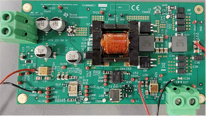
 Figure 3-4 TPS7H5001-SP Push-Pull
Closed-Loop EVM
 Figure 3-5 Push-Pull EVM
Schematics