SLVS432F September   2002  – June 2015 TPS62050 , TPS62051 , TPS62052 , TPS62054 , TPS62056

PRODUCTION DATA.  

  1. Features
  2. Applications
  3. Description
  4. Typical Application Schematic
  5. Revision History
  6. Device Comparison Table
  7. Pin Configuration and Functions
  8. Specifications
    1. 8.1 Absolute Maximum Ratings
    2. 8.2 ESD Ratings
    3. 8.3 Recommended Operating Conditions
    4. 8.4 Thermal Information
    5. 8.5 Electrical Characteristics
    6. 8.6 Typical Characteristics
  9. Detailed Description
    1. 9.1 Overview
    2. 9.2 Functional Block Diagram
    3. 9.3 Feature Description
      1. 9.3.1 Enable and Overtemperature Protection
      2. 9.3.2 Low-Battery Detector (Standard Version)
      3. 9.3.3 ENABLE / Low-Battery Detector (Enhanced Version) TPS62051 Only
      4. 9.3.4 Undervoltage Lockout
      5. 9.3.5 Power Good Comparator
      6. 9.3.6 Synchronization
    4. 9.4 Device Functional Modes
      1. 9.4.1 Soft-Start
      2. 9.4.2 Constant Frequency Mode Operation (SYNC = HIGH)
      3. 9.4.3 Power-Save Mode Operation (SYNC = LOW)
      4. 9.4.4 100% Duty Cycle Low Dropout Operation
      5. 9.4.5 No Load Operation
  10. 10Application and Implementation
    1. 10.1 Application Information
    2. 10.2 Typical Applications
      1. 10.2.1 Standard Circuit for Adjustable Version
        1. 10.2.1.1 Design Requirements
        2. 10.2.1.2 Detailed Design Procedure
          1. 10.2.1.2.1 Inductor Selection
          2. 10.2.1.2.2 Output Capacitor Selection
          3. 10.2.1.2.3 Input Capacitor Selection
          4. 10.2.1.2.4 Feedforward Capacitor
        3. 10.2.1.3 Application Curves
      2. 10.2.2 Standard Circuit for Fixed Voltage Version
        1. 10.2.2.1 Design Requirements
        2. 10.2.2.2 Detailed Design Procedure
        3. 10.2.2.3 Application Curves
    3. 10.3 System Examples
  11. 11Power Supply Recommendations
  12. 12Layout
    1. 12.1 Layout Guidelines
    2. 12.2 Layout Example
  13. 13Device and Documentation Support
    1. 13.1 Device Support
      1. 13.1.1 Third-Party Products Disclaimer
    2. 13.2 Related Links
    3. 13.3 Community Resource
    4. 13.4 Trademarks
    5. 13.5 Electrostatic Discharge Caution
    6. 13.6 Glossary
  14. 14Mechanical, Packaging, and Orderable Information

7 Pin Configuration and Functions

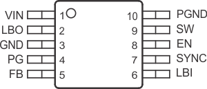
DGS Package
10-Pin VSSOP
Top View
TPS62050 TPS62051 TPS62052 TPS62054 TPS62056 po_lvs432.gif

Pin Functions

PIN I/O DESCRIPTION
NAME NO.
EN 8 I Enable. A logic high enables the converter, logic low forces the device into shutdown mode, reducing the supply current to less than 2 µA.
FB 5 I Feedback pin for the fixed output voltage option. For the adjustable version, an external resistive divider is connected to this pin. The internal voltage divider is disabled for the adjustable version.
GND 3 I Ground
LBI 6 I Low battery input.
LBO 2 O Open-drain low battery output. Logic low signal indicates a low battery voltage.
PG 4 O Power good comparator output. This is an open-drain output. A pullup resistor must be connected between PG and VOUT. The output floats when the output voltage is greater than 95% of the nominal value.
PGND 10 I Power ground. Connect all power grounds to this pin.
SW 9 O Connect the inductor to this pin. This pin is the switch pin and connected to the drain of the internal power MOSFETS.
SYNC 7 I Input for synchronization to the external clock signal. This input can be connected to an external clock or pulled to GND or VI. When an external clock signal is applied, the device synchronizes to this external clock and the device operates in fixed PWM mode. When the pin is pulled to either GND or VI, the internal oscillator is used and the logic level determines if the device operates in fixed PWM or PWM/PFM mode.
SYNC = HIGH: Low-noise mode enabled, fixed-frequency PWM operation is forced.
SYNC = LOW (GND): Power save mode enabled, PFM/PWM mode enabled.
VIN 1 I Supply voltage input.