SLVS503F November   2003  – February 2020 TPS2490 , TPS2491

PRODUCTION DATA.  

  1. Features
  2. Applications
  3. Description
    1.     Device Images
      1.      Typical Application
  4. Revision History
  5. Pin Configuration and Functions
    1.     Pin Functions
  6. Specifications
    1. 6.1 Absolute Maximum Ratings
    2. 6.2 ESD Ratings
    3. 6.3 Recommended Operating Conditions
    4. 6.4 Thermal Information
    5. 6.5 Electrical Characteristics
    6. 6.6 Switching Characteristics
    7. 6.7 Typical Characteristics
  7. Detailed Description
    1. 7.1 Overview
    2. 7.2 Functional Block Diagram
    3. 7.3 Feature Description
      1. 7.3.1  VCC
      2. 7.3.2  SENSE
      3. 7.3.3  GATE
      4. 7.3.4  OUT
      5. 7.3.5  EN
      6. 7.3.6  VREF
      7. 7.3.7  PROG
      8. 7.3.8  TIMER
      9. 7.3.9  PG
      10. 7.3.10 GND
    4. 7.4 Device Functional Modes
      1. 7.4.1 Board Plug-In ()
      2. 7.4.2 TIMER and PG Operation ()
      3. 7.4.3 Action of the Constant Power Engine ()
      4. 7.4.4 Response to a Hard Output Short ( and )
      5. 7.4.5 Automatic Restart ()
  8. Application and Implementation
    1. 8.1 Application Information
      1. 8.1.1 Alternative Inrush Designs
        1. 8.1.1.1 Gate Capacitor (dV/dt) Control
        2. 8.1.1.2 PROG Inrush Control
      2. 8.1.2 Additional Design Considerations
        1. 8.1.2.1 Use of PG
        2. 8.1.2.2 Faults and Backplane Voltage Droop
        3. 8.1.2.3 Output Clamp Diode
        4. 8.1.2.4 Gate Clamp Diode
        5. 8.1.2.5 High Gate Capacitance Applications
        6. 8.1.2.6 Input Bypass
        7. 8.1.2.7 Output Short Circuit Measurements
    2. 8.2 Typical Application
      1. 8.2.1 Design Requirements
      2. 8.2.2 Detailed Design Procedure
        1. 8.2.2.1 Select RSNS and CL setting
        2. 8.2.2.2 Selecting the Hot Swap FET(s)
        3. 8.2.2.3 Select Power Limit
        4. 8.2.2.4 Set Fault Timer
        5. 8.2.2.5 Check MOSFET SOA
        6. 8.2.2.6 Set Under-Voltage Threshold
        7. 8.2.2.7 Choose R5, and CIN
        8. 8.2.2.8 Input and Output Protection
        9. 8.2.2.9 Final Schematic and Component Values
      3. 8.2.3 Application Curves
  9. Power Supply Recommendations
  10. 10Layout
    1. 10.1 Layout Guidelines
      1. 10.1.1 PC Board Guidelines
      2. 10.1.2 System Considerations
    2. 10.2 Layout Example
  11. 11Device and Documentation Support
    1. 11.1 Development Support
    2. 11.2 Documentation Support
      1. 11.2.1 Related Documentation
    3. 11.3 Related Links
    4. 11.4 Receiving Notification of Documentation Updates
    5. 11.5 Community Resources
    6. 11.6 Trademarks
    7. 11.7 Electrostatic Discharge Caution
    8. 11.8 Glossary
  12. 12Mechanical, Packaging, and Orderable Information

Select RSNS and CL setting

The TPS2490 monitors the current in the external MOSFET (Q1) by measuring the voltage across the sense resistor (RS), connected from VIN to SENSE. When the voltage difference across the Vin and Sense pins (VCL) is greater than 50 mV(typical), the LM5069 will begin regulating the MOSFET gate. Size RSNS for maximum or minimum VCL for applications that require guaranteed shutoff or guaranteed conduction. In this design example, RSNS is sized to exhibit minimum VCL across RSNS at maximum load current.

Equation 6. TPS2490 TPS2491 tps2490_equation1.gif

Typically sense resistors are only available in discrete values. If a precise current limit is desired, a sense resistor along with a resistor divider can be used as shown in Figure 19.
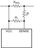
TPS2490 TPS2491 TPS2490_ResDiv.gifFigure 19. SENSE Resistor Divider

If using a resistor divider, then the next larger available sense resistor should be chosen (1 mΩ for example). The ratio of R1 and R2 can then be computed as follows:

Equation 7. TPS2490 TPS2491 tps2490_equation2.gif

Note that the SENSE pin typically pulls 7.5 µA of current, which creates an offset across R2. TI recommends to keep R2 below 10 Ω to reduce the offset that this introduces. In addition the 1% resistors add to the current monitoring error. Finally, if the resistor divider approach is used, the user should compute the effective sense resistance (RSNS,EFF) using Equation 8 instead of RSNS in all equations.

Equation 8. TPS2490 TPS2491 tps2490_equation3.gif

Note that for many applications, a precise current limit may not be required. In that case, it is simpler to pick the next smaller available sense resistor. For this application, a resistive divider was not used, and a 4 mΩ resistor was used for a 12.5 A (typical) current limit.