SLVS651B May 2006 – December 2015 TPS62510
PRODUCTION DATA.
- 1 Features
- 2 Applications
- 3 Description
- 4 Revision History
- 5 Pin Configuration and Functions
- 6 Specifications
- 7 Detailed Description
- 8 Application and Implementation
- 9 Power Supply Recommendations
- 10Layout
- 11Device and Documentation Support
- 12Mechanical, Packaging, and Orderable Information
5 Pin Configuration and Functions
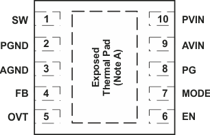
DRC Package
10-Pin VSON
Top View

The exposed thermal pad is connected to AGND.
Pin Functions
| PIN | I/O | DESCRIPTION | |
|---|---|---|---|
| NAME | NO. | ||
| SW | 1 | — | Switch pin of the converter. The inductor is connected here. |
| PGND | 2 | — | Power ground for the converter |
| AGND | 3 | — | Analog ground connection |
| FB | 4 | I | Feedback voltage sense input. Connect directly to VOUT or to the midpoint of an external voltage divider for the adjustable version. |
| OVT | 5 | I | Output voltage tracking input. The signal applied to this pin is used as reference voltage overriding the internal reference voltage when it is below the internal 0.6-V reference. If this feature is not used, the OVT pin is connected to VIN. |
| EN | 6 | I | Enable pin. A logic high enables the regulator, a logic low disables the regulator. This pin needs to be terminated and not left floating. |
| MODE | 7 | I | This pin is used to force fixed frequency PWM operation or to synchronize the device to an external clock signal. With MODE = High, the device is forced into 1.5-MHz fixed frequency PWM operation. With MODE = Low, the device automatically enters the power save mode at light load currents. |
| PG | 8 | O | Power good indication. This is a open drain output that is low when the device is disabled or the output voltage drops 10% below target. |
| AVIN | 9 | — | Power supply for control circuitry. Must be connected to the same voltage supply as PVIN through RC filter. |
| PVIN | 10 | — | Input voltage for the power stage. VIN must be connected to the same voltage supply as AVIN. |
| Exposed Thermal Pad | C2 | — | Connect the exposed thermal pad to analog ground AGND. |