7 Specifications
7.1 Absolute Maximum Ratings
over operating free–air temperature range (unless otherwise noted)(1)
|
MIN |
MAX |
UNIT |
| VIN, ON |
Input voltage |
–0.3 |
4 |
V |
| VOUT |
Output voltage |
–0.3 |
4 |
V |
| IMAX |
Maximum continuous switch current at TA = 60°C |
|
3 |
A |
| IPLS |
Maximum pulsed switch current, 100–μs pulse, 2% duty cycle |
|
4 |
A |
| TJ |
Junction temperature |
|
125 |
°C |
| Tstg |
Storage temperature |
–65 |
150 |
°C |
(1) Stresses beyond those listed under Absolute Maximum Ratings may cause permanent damage to the device. These are stress ratings only, which do not imply functional operation of the device at these or any other conditions beyond those indicated under Recommended Operating Conditions. Exposure to absolute–maximum–rated conditions for extended periods may affect device reliability.
7.2 ESD Ratings
|
VALUE |
UNIT |
| V(ESD) |
Electrostatic discharge |
Human–body model (HBM), per ANSI/ESDA/JEDEC JS–001(1) |
±2000 |
V |
| Charged–device model (CDM), per JEDEC specification JESD22–C101(2) |
±1000 |
(1) JEDEC document JEP155 states that 500–V HBM allows safe manufacturing with a standard ESD control process. Manufacturing with less than 500–V HBM is possible with the necessary precautions.
(2) JEDEC document JEP157 states that 250–V CDM allows safe manufacturing with a standard ESD control process. Manufacturing with less than 250–V CDM is possible with the necessary precautions.
7.3 Recommended Operating Conditions
over operating free-air temperature range (unless otherwise noted)
|
MIN |
MAX |
UNIT |
| VIN |
Input voltage |
0.65 |
3.6 |
V |
| VOUT |
Output voltage |
0 |
3.6 |
V |
| VIH |
High–level input voltage, ON |
0.9 |
3.6 |
V |
| VIL |
Low–level input voltage, ON |
0 |
0.45 |
V |
| CIN |
Input capacitance |
1 |
|
µF |
| TA |
Operating free–air temperature |
–40 |
105 |
°C |
7.4 Thermal Information
| THERMAL METRIC(1) |
TPS22925xx |
UNIT |
| YPH (DSBGA) |
| 6 PINS |
| RθJA |
Junction–to–ambient thermal resistance |
110.9 |
°C/W |
| RθJC(top) |
Junction–to–case (top) thermal resistance |
1.2 |
°C/W |
| RθJB |
Junction–to–board thermal resistance |
30.4 |
°C/W |
| ψJT |
Junction–to–top characterization parameter |
0.8 |
°C/W |
| ψJB |
Junction–to–board characterization parameter |
30.4 |
°C/W |
(1) For more information about traditional and new thermal metrics, see the
Semiconductor and IC Package Thermal Metrics application report,
SPRA953.
7.5 Electrical Characteristics
over operating free–air temperature range (unless otherwise noted). Typical values are for TA = 25°C.
| PARAMETER |
TEST CONDITIONS |
TA |
MIN |
TYP |
MAX |
UNIT |
| IQ,VIN |
Quiescent current |
VON = 3.6 V,
IOUT = 0 A |
VIN = 3.6 V |
–40°C to +85°C |
|
29 |
71 |
µA |
| –40°C to +105°C |
|
|
84 |
| VIN = 2.5 V |
–40°C to +85°C |
|
28 |
67 |
| –40°C to +105°C |
|
|
79 |
| VIN = 1.8 V |
–40°C to +85°C |
|
26 |
65 |
| –40°C to +105°C |
|
|
76 |
| VIN = 1.2 V |
–40°C to +85°C |
|
20 |
55 |
| –40°C to +105°C |
|
|
66 |
| VIN = 1 V |
–40°C to +85°C |
|
16 |
50 |
| –40°C to +105°C |
|
|
60 |
| VIN = 0.65 V |
–40°C to +85°C |
|
10 |
39 |
| –40°C to +105°C |
|
|
49 |
| ISD,VIN |
VIN shutdown current |
VON = 0 V,
VOUT = 0 V |
VIN = 3.6 V |
–40°C to +85°C |
|
0.5 |
5 |
µA |
| –40°C to +105°C |
|
|
9 |
| VIN = 2.5 V |
–40°C to +85°C |
|
0.5 |
4 |
| –40°C to +105°C |
|
|
6 |
| VIN = 1.8 V |
–40°C to +85°C |
|
0.5 |
4 |
| –40°C to +105°C |
|
|
6 |
| VIN = 1.2 V |
–40°C to +85°C |
|
0.5 |
3 |
| –40°C to +105°C |
|
|
5 |
| VIN = 1 V |
–40°C to +85°C |
|
0.5 |
3 |
| –40°C to +105°C |
|
|
5 |
| VIN = 0.65 V |
–40°C to +85°C |
|
0.5 |
3 |
| –40°C to +105°C |
|
|
5 |
| ION |
ON pin input leakage current |
0.9 V ≤ VON ≤ 3.6 V |
–40°C to +105°C |
|
|
0.1 |
µA |
| IRC,VIN |
Reverse current when disabled |
VIN = VON = 0 V, VOUT = 3.6 V |
–40°C to +85°C |
|
–0.2 |
–2.5 |
µA |
| –40°C to +105°C |
|
|
–6 |
| RON |
On-resistance |
IOUT = –200 mA |
VIN = 3.6 V |
25°C |
|
9.2 |
13 |
mΩ |
| –40°C to +85°C |
|
|
15 |
| –40°C to +105°C |
|
|
16 |
| VIN = 2.5 V |
25°C |
|
9.2 |
13 |
| –40°C to +85°C |
|
|
15 |
| –40°C to +105°C |
|
|
16 |
| VIN = 1.8 V |
25°C |
|
9.2 |
13 |
| –40°C to +85°C |
|
|
15 |
| –40°C to +105°C |
|
|
16 |
| VIN = 1.2 V |
25°C |
|
9.5 |
14 |
| –40°C to +85°C |
|
|
16 |
| –40°C to +105°C |
|
|
17 |
| VIN = 1 V |
25°C |
|
10.2 |
15 |
| –40°C to +85°C |
|
|
17 |
| –40°C to +105°C |
|
|
18 |
| VIN = 0.65 V |
25°C |
|
13.1 |
20 |
| –40°C to +85°C |
|
|
23 |
| –40°C to +105°C |
|
|
25 |
| VHYS |
ON pin hysteresis |
VIN = 3.6 V |
25°C |
|
86 |
|
mV |
| VIN = 2.5 V |
|
83 |
|
| VIN = 1.8 V |
|
82 |
|
| VIN = 1.2 V |
|
80 |
|
| VIN = 1 V |
|
79 |
|
| VIN = 0.65 V |
|
79 |
|
| RPD(1) |
Output pull-down resistance |
VIN = VOUT = 3.6 V,
VON = 0 V |
–40°C to +85°C |
|
150 |
205 |
Ω |
| –40°C to +105°C |
|
|
215 |
(1) Applies to TPS22925B and TPS22925C only.
7.6 Switching Characteristics(1)
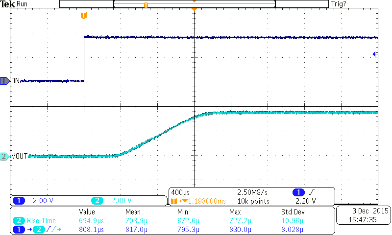
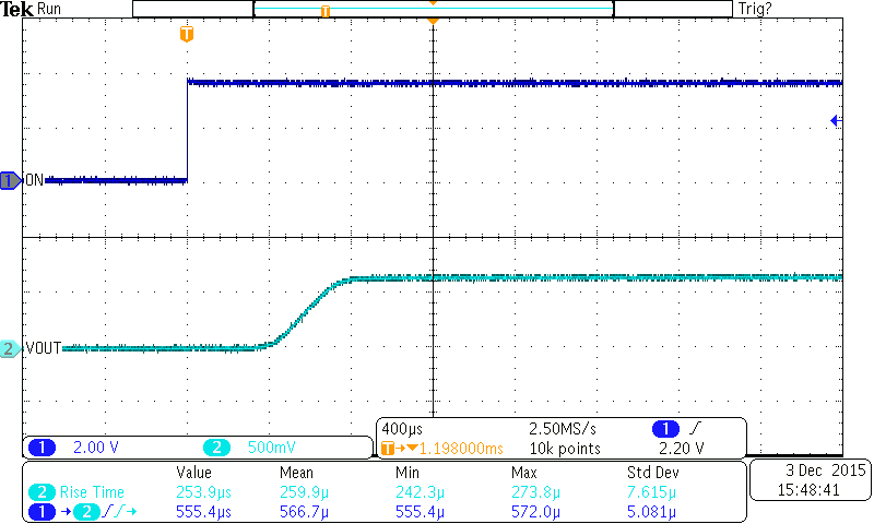
over operating free-air temperature range (unless otherwise noted) VON = 3.6 V, RL = 10 Ω, CIN = 1 µF, CL = 0.1 µF,TA = 25°C
| PARAMETER |
TEST CONDITIONS |
TYP
(TPS22925Bx) |
TYP
(TPS22925Cx) |
UNIT |
| tON |
Turnon time |
VIN = 3.6 V |
110 |
900 |
µs |
| VIN = 1.8 V |
94 |
730 |
| VIN = 0.65 V |
86 |
620 |
| tOFF |
Turnoff time |
VIN = 3.6 V |
3 |
3 |
µs |
| VIN = 1.8 V |
2.7 |
2.7 |
| VIN = 0.65 V |
10.9 |
10.9 |
| tR |
Output voltage rise time |
VIN = 3.6 V |
97 |
810 |
µs |
| VIN = 1.8 V |
61 |
520 |
| VIN = 0.65 V |
36 |
300 |
| tF |
Output voltage fall time |
VIN = 3.6 V |
2.2 |
2.2 |
µs |
| VIN = 1.8 V |
2.1 |
2.1 |
| VIN = 0.65 V |
3.6 |
3.6 |
| tD |
Delay time |
VIN = 3.6 V |
64 |
500 |
µs |
| VIN = 1.8 V |
66 |
490 |
| VIN = 0.65 V |
68 |
470 |
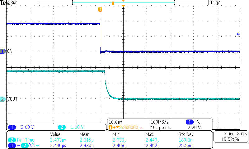
(1) Turn-off time and fall time are dependent on the time constant at the load. For TPS22925BN and TPS22925CN, there is no QOD. The time constant is RL× CL. For TPS22925B and TPS22925C, internal pull-down resistor RPD is enabled when the switch is disabled. The time constant is (RPD || RL) × CL.
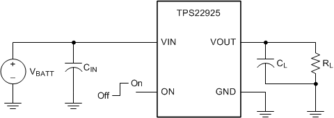 Figure 1. Timing Test Circuit

Rise times and fall times of the control signal is 100 ns.
Figure 2. Timing Waveforms
7.7 Typical Characteristics
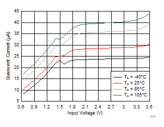
 Figure 3. Quiescent Current vs Input Voltage

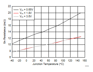
| VON = 3.6 V |
IOUT = –200 mA |
Figure 5. On-Resistance vs Temperature

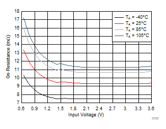
| VON = 3.6 V |
IOUT = –200 mA |
Figure 7. On-Resistance vs Input Voltage
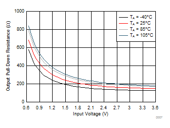
 Figure 9. Output Pull-Down Resistance vs Input Voltage
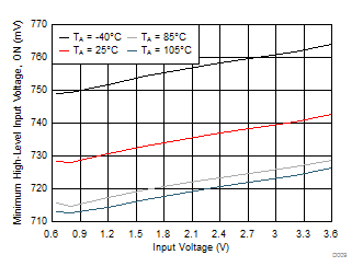
 Figure 11. High-Level Input Voltage vs Input Voltage

| VON rising from 0 V to 3.6 V |
CIN = 1 μF |
| CL = 0.1 μF |
RL = 10 Ω |
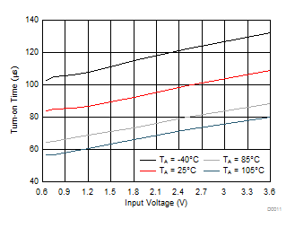
Figure 13. Turn-on Time vs Input Voltage (TPS22925Bx)

| VON falling from 3.6 V to 0 V |
CIN = 1 μF |
| CL = 0.1 μF |
RL = 10 Ω |
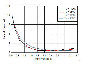
Figure 15. Turn-Off Time vs Input Voltage

| VON rising from 0 V to 3.6 V |
CIN = 1 μF |
| CL = 0.1 μF |
RL = 10 Ω |
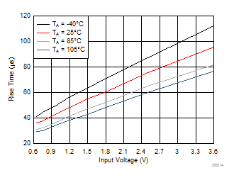
Figure 17. Rise Time vs Input Voltage (TPS22925Cx)

| VON rising from 0 V to 3.6 V |
CIN = 1 μF |
| CL = 0.1 μF |
RL = 10 Ω |
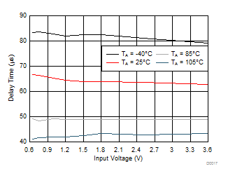
Figure 19. Delay Time vs Input Voltage (TPS22925Bx)
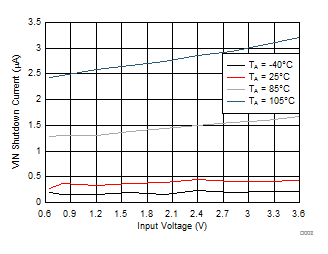
 Figure 4. Input Shutdown Current vs Input Voltage
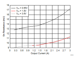
 Figure 6. On-Resistance vs Output Current
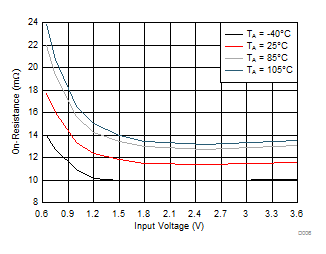
 Figure 8. On-Resistance vs Input Voltage
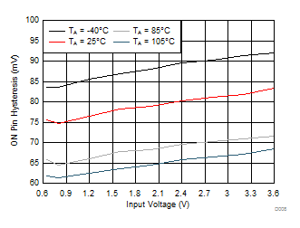
 Figure 10. Hysteresis vs Input Voltage
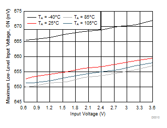
 Figure 12. Low-Level Input Voltage vs Input Voltage

| VON rising from 0 V to 3.6 V |
CIN = 1 μF |
| CL = 0.1 μF |
RL = 10 Ω |
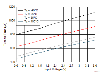
Figure 14. Turn-On Time vs Input Voltage (TPS22925Cx)

| VON rising from 0 V to 3.6 V |
CIN = 1 μF |
| CL = 0.1 μF |
RL = 10 Ω |
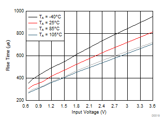
Figure 16. Rise Time vs Input Voltage (TPS22925Bx)

| VON falling from 3.6 V to 0 V |
CIN = 1 μF |
| CL = 0.1 μF |
RL = 10 Ω |
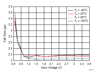
Figure 18. Fall Time vs Input Voltage

| VON rising from 0 V to 3.6 V |
CIN = 1 μF |
| CL = 0.1 μF |
RL = 10 Ω |
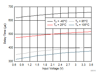
Figure 20. Delay Time vs Input Voltage (TPS22925Cx)
7.8 Typical Characteristics
CIN = 1 μF, CL = 0.1 μF, RL = 10 Ω, TA = 25°C
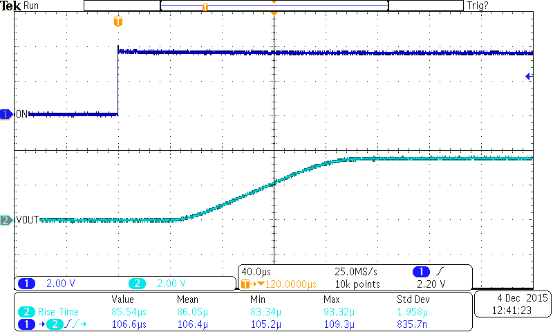
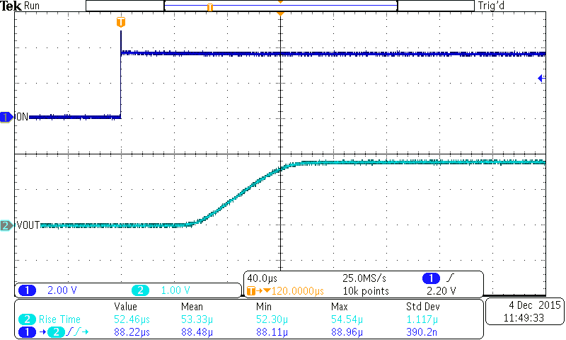
 Figure 21. Turnon Response (TPS22925Bx)
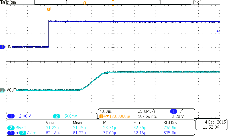
 Figure 23. Turnon Response (TPS22925Bx)
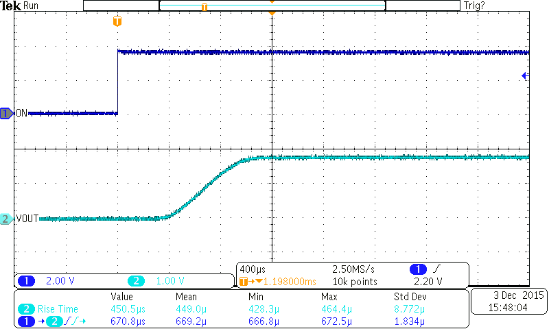
 Figure 25. Turnon Response (TPS22925Cx)
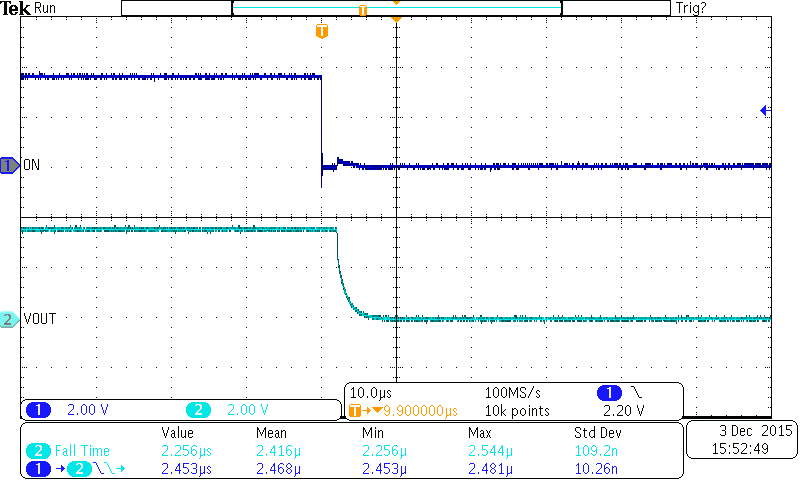
 Figure 27. Turnoff Response (TPS22925xx)
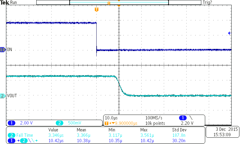
 Figure 29. Turnoff Response (TPS22925xx)
 Figure 22. Turnon Response (TPS22925Bx)
 Figure 24. Turnon Response (TPS22925Cx)
 Figure 26. Turnon Response (TPS22925Cx)
 Figure 28. Turnoff Response (TPS22925xx)
 Figure 1. Timing Test Circuit

