SLVSAC4B November 2010 – December 2015 TLV62065
PRODUCTION DATA.
- 1 Features
- 2 Applications
- 3 Description
- 4 Revision History
- 5 Pin Configuration and Functions
- 6 Specifications
- 7 Detailed Description
- 8 Application and Implementation
- 9 Power Supply Recommendations
- 10Layout
- 11Device and Documentation Support
- 12Mechanical, Packaging, and Orderable Information
8 Application and Implementation
NOTE
Information in the following applications sections is not part of the TI component specification, and TI does not warrant its accuracy or completeness. TI’s customers are responsible for determining suitability of components for their purposes. Customers should validate and test their design implementation to confirm system functionality.
8.1 Application Information
The TLV62065 is a high-efficiency synchronous step-down DC/DC converter providing up to 2-A output current.
8.2 Typical Application
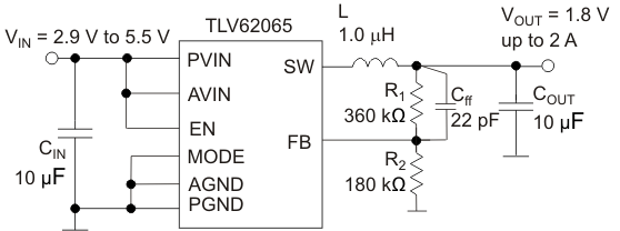 Figure 8. TLV62065 1.8-V Adjustable Output Voltage Configuration
8.2.1 Design Requirements
The device operates over an input voltage range from 2.9 V to 5.5 V. The output voltage is adjustable using an external feedback divider.
8.2.2 Detailed Design Procedure
8.2.2.1 Output Voltage Setting
The output voltage can be calculated by Equation 2 with an internal reference voltage VREF typically 0.6 V.

To minimize the current through the feedback divider network, R2 should be within the range of 120 kΩ to 360 kΩ. The sum of R1 and R2 should not exceed approximately 1 MΩ, to keep the network robust against noise. An external feed-forward capacitor Cff is required for optimum regulation performance. Lower resistor values can be used. R1 and Cff places a zero in the loop. The right value for Cff can be calculated by Equation 3 and Equation 4:


8.2.2.2 Output Filter Design (Inductor and Output Capacitor)
The internal compensation network of TLV62065 is optimized for a LC output filter with a corner frequency of:
The device operates with nominal inductors of 1.0 µH to 1.2 µH and with 10 µF to 22 µF small X5R and X7R ceramic capacitors. Please refer to the lists of inductors and capacitors. The device is optimized for a 1-µH inductor and 10-µF output capacitor.
8.2.2.2.1 Inductor Selection
The inductor value has a direct effect on the ripple current. The selected inductor has to be rated for its DC resistance and saturation current. The inductor ripple current (ΔIL) decreases with higher inductance and increases with higher VI or VO.
Equation 5 calculates the maximum inductor current in PWM mode under static load conditions. The saturation current of the inductor should be rated higher than the maximum inductor current as calculated with Equation 6. This is recommended because during heavy load transient the inductor current rises above the calculated value.


where
- f = Switching frequency (3 MHz typical)
- L = Inductor value
- ΔIL = Peak-to-peak inductor ripple current
- ILmax = Maximum inductor current
A more conservative approach is to select the inductor current rating just for the switch current limit ILIMF of the converter.
The total losses of the coil have a strong impact on the efficiency of the DC–DC conversion and consist of both the losses in the DC resistance R(DC) and the following frequency-dependent components:
- The losses in the core material (magnetic hysteresis loss, especially at high switching frequencies)
- Additional losses in the conductor from the skin effect (current displacement at high frequencies)
- Magnetic field losses of the neighboring windings (proximity effect)
- Radiation losses
Table 1. List of Inductors
| DIMENSIONS [mm3] | INDUCTANCE μH | INDUCTOR TYPE | SUPPLIER |
|---|---|---|---|
| 3.2 x 2.5 x 1.0 max | 1.0 | LQM32PN (MLCC) | Murata |
| 3.7 x 4 x 1.8 max | 1.0 | LQH44 (wire wound) | Murata |
| 4.0 x 4.0 x 2.6 max | 1.2 | NRG4026T (wire wound) | Taiyo Yuden |
| 3.5 x 3.7 x 1.8 max | 1.2 | DE3518 (wire wound) | TOKO |
8.2.2.2.2 Output Capacitor Selection
The advanced fast-response voltage mode control scheme of the TLV62065 allows the use of tiny ceramic capacitors. Ceramic capacitors with low ESR values have the lowest output voltage ripple and are recommended. The output capacitor requires either an X7R or X5R dielectric. Y5V and Z5U dielectric capacitors, aside from their wide variation in capacitance over temperature, become resistive at high frequencies and may not be used. For most applications a nominal 10-µF or 22-µF capacitor is suitable. At small ceramic capacitors, the DC-bias effect decreases the effective capacitance. Therefore a 22-µF capacitor can be used for output voltages higher than 2 V, see list of capacitors.
In case additional ceramic capacitors in the supplied system are connected to the output of the DC–DC converter, the output capacitor COUT need to be decreased in order not to exceed the recommended effective capacitance range. In this case a loop stability analysis must be performed as described later.
At nominal load current, the device operates in PWM mode and the RMS ripple current is calculated by Equation 7:

8.2.2.2.3 Input Capacitor Selection
Because of the nature of the buck converter having a pulsating input current, a low ESR input capacitor is required for best input voltage filtering and minimizing the interference with other circuits caused by high input voltage spikes. For most applications a 10-µF ceramic capacitor is recommended. The input capacitor can be increased without any limit for better input voltage filtering.
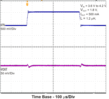
Take care when using only small ceramic input capacitors. When a ceramic capacitor is used at the input and the power is being supplied through long wires, such as from a wall adapter, a load step at the output or VIN step on the input can induce ringing at the VIN pin. This ringing can couple to the output and be mistaken as loop instability or could even damage the part by exceeding the maximum ratings.
Table 2. List of Capacitors
| CAPACITANCE | TYPE | SIZE [ mm3] | SUPPLIER |
|---|---|---|---|
| 10 μF | GRM188R60J106M | 0603: 1.6 x 0.8 x 0.8 | Murata |
| 22 μF | GRM188R60G226M | 0603: 1.6 x 0.8 x 0.8 | Murata |
| 22 µF | CL10A226MQ8NRNC | 0603: 1.6 x 0.8 x 0.8 | Samsung |
| 10 µF | CL10A106MQ8NRNC | 0603: 1.6 x 0.8 x 0.8 | Samsung |
8.2.2.3 Checking Loop Stability
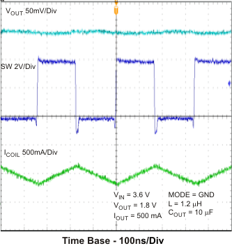
The first step of circuit and stability evaluation is to look from a steady-state perspective at the following signal:
- Switching node, SW
- Inductor current, IL
- Output ripple voltage, VOUT(AC)
These are the basic signals that need to be measured when evaluating a switching converter. When the switching waveform shows large duty cycle jitter or the output voltage or inductor current shows oscillations, the regulation loop may be unstable. This is often a result of board layout and/or wrong L-C output filter combinations. As a next step in the evaluation of the regulation loop, the load transient response is tested. The time between the application of the load transient and the turn on of the P-channel MOSFET, the output capacitor must supply all of the current required by the load. VOUT immediately shifts by an amount equal to ΔI(LOAD) x ESR, where ESR is the effective series resistance of COUT. ΔI(LOAD) begins to charge or discharge COUT generating a feedback error signal used by the regulator to return VOUT to its steady-state value. The results are most easily interpreted when the device operates in PWM mode at medium to high load currents.
During this recovery time, VOUT can be monitored for settling time, overshoot, or ringing; that helps evaluate stability of the converter. Without any ringing, the loop has usually more than 45° of phase margin.
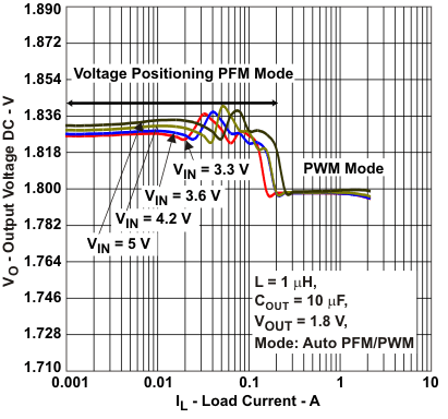
8.2.3 Application Curves
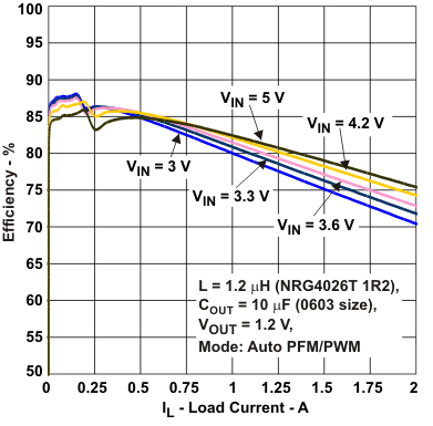
| VOUT = 1.2 V |
Linear Scale
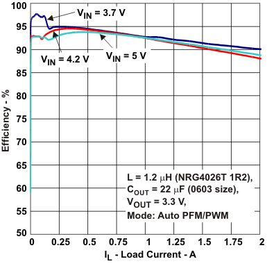
| VOUT = 3.3 V |
Linear Scale
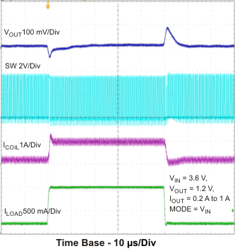
PWM Mode 0.2 A to 1A
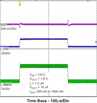
200 mA to 1500 mA
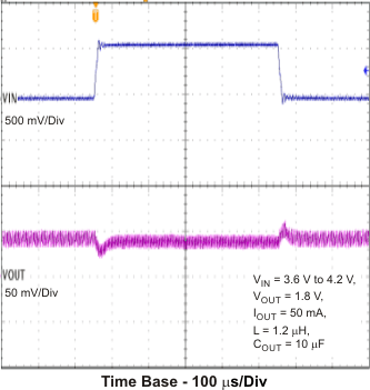
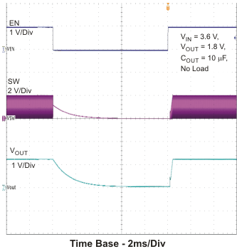
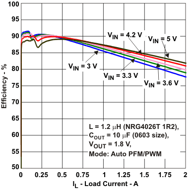
| VOUT = 1.8 V |
Linear Scale
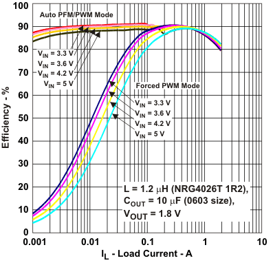
Logarithmic Scale
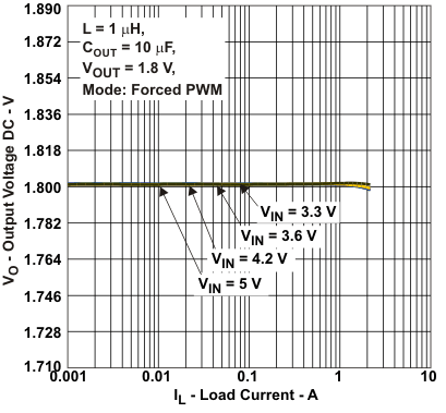
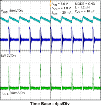
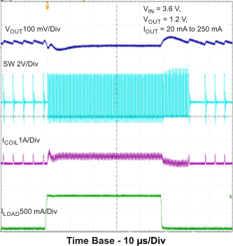
PFM Mode 20 mA to 250 mA
