SLVSAG8G September 2011 – June 2016 TPS612592
UNLESS OTHERWISE NOTED, this document contains PRODUCTION DATA.
- 1 Features
- 2 Applications
- 3 Description
- 4 Revision History
- 5 Device Options
- 6 Pin Configuration and Functions
- 7 Specifications
- 8 Parameter Measurement Information
- 9 Detailed Description
- 10Application and Implementation
- 11Power Supply Recommendations
- 12Layout
- 13Device and Documentation Support
- 14Mechanical, Packaging, and Orderable Information
7 Specifications
7.1 Absolute Maximum Ratings
over operating free-air temperature range (unless otherwise noted)(1)| MIN | MAX | UNIT | ||
|---|---|---|---|---|
| Input voltage | Voltage at VIN(2), VOUT(2), SW(2), EN(2), BP(2) | –0.3 | 7 | V |
| Input current | Continuous average current into SW (4) | 1.8 | A | |
| Peak current into SW (5) | 3.5 | |||
| Power dissipation | Internally limited | |||
| Temperature | Operating, TA (3) | –40 | 85 | °C |
| Operating virtual junction, TJ | –40 | 150 | ||
| Storage, Tstg | –65 | 150 | ||
(1) Stresses beyond those listed under absolute maximum ratings may cause permanent damage to the device. These are stress ratings only, and functional operation of the device at these or any other conditions beyond those indicated under recommended operating conditions is not implied. Exposure to absolute-maximum-rated conditions for extended periods my affect device reliability.
(2) All voltages are with respect to network ground terminal.
(3) In applications where high power dissipation and/or poor package thermal resistance is present, the maximum ambient temperature may have to be derated. Maximum ambient temperature (TA(max)) is dependent on the maximum operating junction temperature (TJ(max)), the maximum power dissipation of the device in the application (PD(max)), and the junction-to-ambient thermal resistance of the part/package in the application (θJA), as given by the following equation: TA(max)= TJ(max)–(θJA X PD(max)). To achieve optimum performance, it is recommended to operate the device with a maximum junction temperature of 105°C.
(4) Limit the junction temperature to 105°C for continuous operation at maximum output power.
(5) Limit the junction temperature to 125°C for 5% duty cycle operation.
7.2 ESD Ratings
| VALUE | UNIT | |||
|---|---|---|---|---|
| V(ESD) | Electrostatic discharge | Human-body model (HBM), per ANSI/ESDA/JEDEC JS-001(1) | ±2000 | V |
| Charged-device model (CDM), per JEDEC specification JESD22-C101(2) | ±1000 | |||
| Machine model (MM) | ±200 | |||
(1) JEDEC document JEP155 states that 500-V HBM allows safe manufacturing with a standard ESD control process. Manufacturing with less than 500-V HBM is possible with the necessary precautions.
(2) JEDEC document JEP157 states that 250-V CDM allows safe manufacturing with a standard ESD control process. Manufacturing with less than 250-V CDM is possible with the necessary precautions.
7.3 Recommended Operating Conditions
| MIN | NOM | MAX | UNIT | |||
|---|---|---|---|---|---|---|
| VI | Input voltage range | TPS61253 | 2.65(1) | 4.85 | V | |
| TPS61254 | 2.5 | 4.35 | ||||
| TPS61256 | 2.5 | 4.85 | ||||
| TPS61257 | 2.5 | 4.15 | ||||
| TPS61258 | 2.65(1) | 4.35 | ||||
| TPS61259 | 2.65(1) | 4.85 | ||||
| TPS612592 | 2.65(1) | 4.85 | ||||
| RL | Minimum resistive load for start-up | TPS6125x | 55 | Ω | ||
| L | Inductance | 0.7 | 1.0 | 2.9 | µH | |
| CO | Output capacitance | 3.5 | 5 | 50 | µF | |
| TA | Ambient temperature | –40 | 85 | °C | ||
| TJ | Operating junction temperature | –40 | 125 | °C | ||
(1) Up to 1000mA peak output current.
7.4 Thermal Information
| THERMAL METRIC(1) | TPS6125x | UNIT | |
|---|---|---|---|
| YFF | |||
| 9 PINS | |||
| RθJA | Junction-to-ambient thermal resistance | 108.3 | °C/W |
| RθJC(top) | Junction-to-case (top) thermal resistance | 1.0 | |
| RθJB | Junction-to-board thermal resistance | 18 | |
| ψJT | Junction-to-top characterization parameter | 4.2 | |
| ψJB | Junction-to-board characterization parameter | 17.9 | |
(1) For more information about traditional and new thermal metrics, see the Semiconductor and IC Package Thermal Metrics application report.
7.5 Electrical Characteristics
Minimum and maximum values are at VIN = 2.3V to 5.5V, EN = 1.8V, TA = –40°C to 85°C; Circuit of Parameter Measurement Information section (unless otherwise noted). Typical values are at VIN = 3.6V, EN = 1.8V, TA = 25°C (unless otherwise noted).7.6 Typical Characteristics
Table 1. Table of Graphs
| FIGURE | |||
|---|---|---|---|
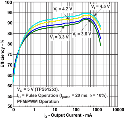
| η | Efficiency | vs Output current | Figure 1, Figure 2, Figure 3, Figure 5 |
| vs Input voltage | Figure 4 | ||
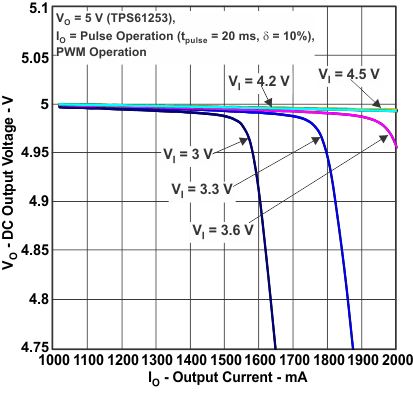
| VO | DC output voltage | vs Output current | Figure 6, Figure 7, Figure 8, Figure 9, Figure 10, Figure 14 |
| vs Input voltage | Figure 11 | ||
| IO | Maximum output current | vs Input voltage | Figure 12, Figure 13 |
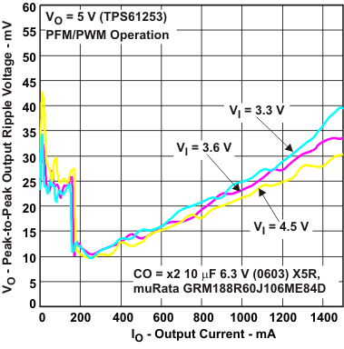
| ΔVO | Peak-to-peak output ripple voltage | vs Output current | Figure 15, Figure 16, Figure 17 |
| ICC | Supply current | vs Input voltage | Figure 18, Figure 19 |
| ILIM | DC pre-charge current | vs Differential input-output voltage | Figure 20, Figure 21 |
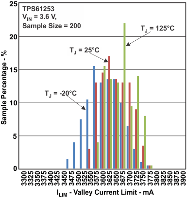
| Valley current limit | vs Temperature | Figure 22, Figure 23 | |
| rDS(on) | MOSFET rDS(on) | vs Temperature | Figure 24 |
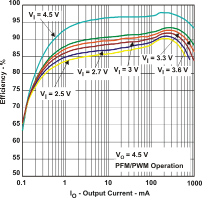 Figure 1. Efficiency vs Output Current
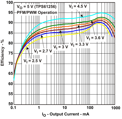 Figure 2. Efficiency vs Output Current
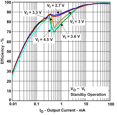 Figure 5. Efficiency vs Output Current
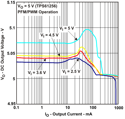 Figure 7. DC Output Voltage vs Output Current
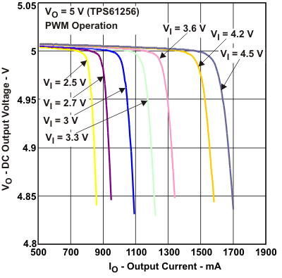 Figure 9. DC Output Voltage vs Output Current
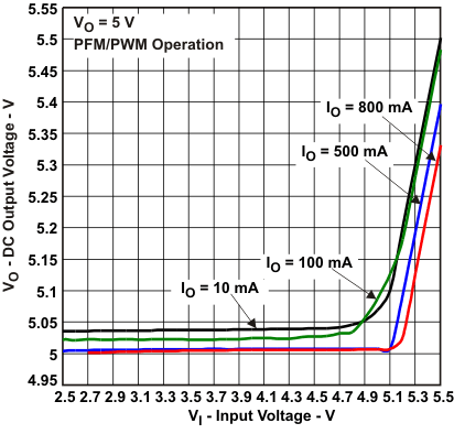 Figure 11. DC Output Voltage vs Input Voltage
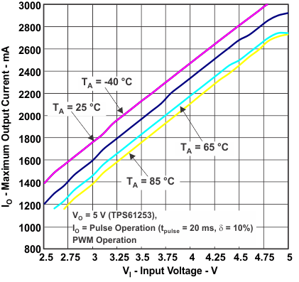 Figure 13. Maximum Output Current vs Input Voltage
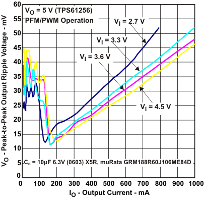 Figure 15. Peak-to-Peak Output Ripple Voltage vs Output Current
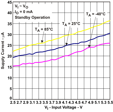 Figure 19. Supply Current vs Input Voltage
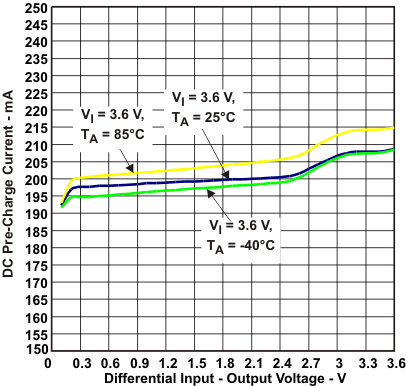 Figure 21. DC Pre-Charge Current vs Differential Input-Output Voltage
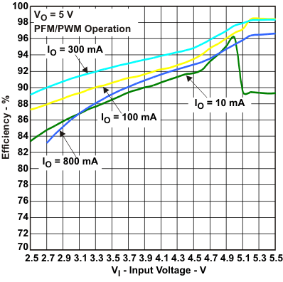 Figure 4. Efficiency vs Input Voltage
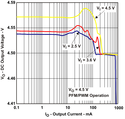 Figure 6. DC Output Voltage vs Output Current
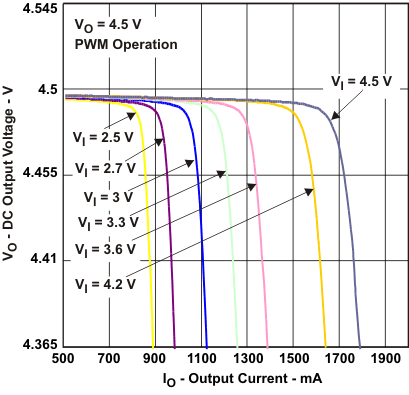 Figure 8. DC Output Voltage vs Output Current
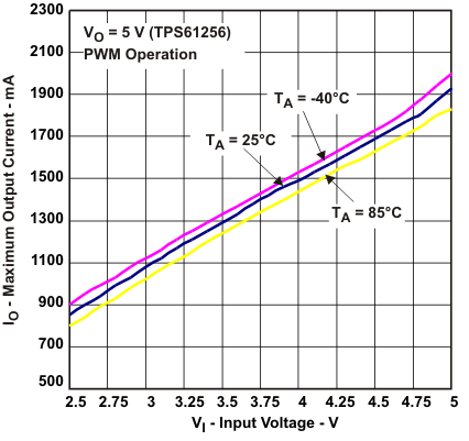 Figure 12. Maximum Output Current vs Input Voltage
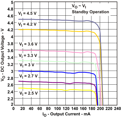 Figure 14. DC Output Voltage vs Output Current
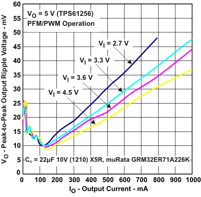 Figure 16. Peak-to-Peak Output Ripple Voltage vs Output Current
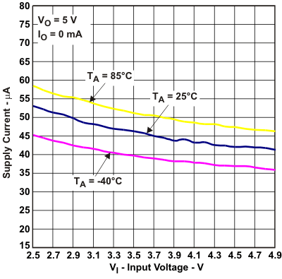 Figure 18. Supply Current vs Input Voltage
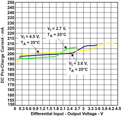 Figure 20. DC Pre-Charge Current vs Differential Input-Output Voltage
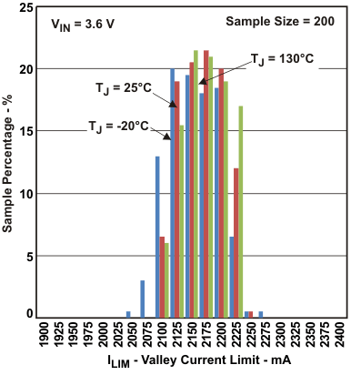 Figure 22. Valley Current Limit
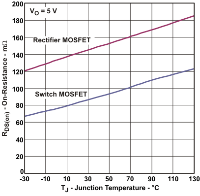 Figure 24. MOSFET rDS(on) vs Temperature
