SLVSAN6B February 2011 – September 2016
PRODUCTION DATA.
- 1 Features
- 2 Applications
- 3 Description
- 4 Revision History
- 5 Device Comparison Table
- 6 Pin Configuration and Functions
- 7 Specifications
- 8 Detailed Description
- 9 Application and Implementation
- 10Power Supply Recommendations
- 11Layout
- 12Device And Documentation Support
- 13Mechanical, Packaging, and Orderable Information
9 Application and Implementation
NOTE
Information in the following applications sections is not part of the TI component specification, and TI does not warrant its accuracy or completeness. TI’s customers are responsible for determining suitability of components for their purposes. Customers should validate and test their design implementation to confirm system functionality.
9.1 Application Information
The TPS61176 provides a high-performance LED lighting solution for tablets, notebooks and other low power LCD backlit displays. The device can drive 6 strings of 10 series LEDs in a compact and high efficient solution. The LED current is controlled via a logic level PWM input and the LED current level is set using an ISET resistor.
9.2 Typical Application
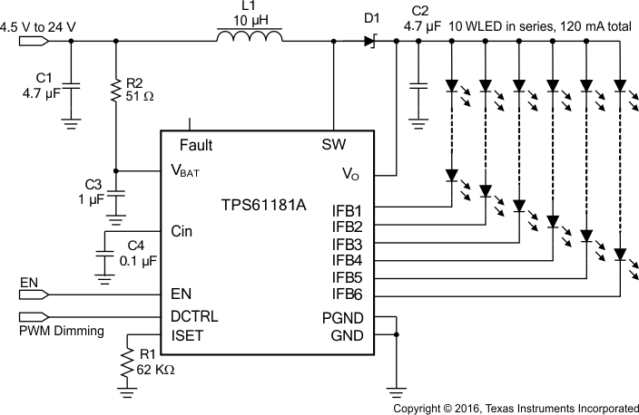 Figure 9. TPS61181A Typical Application
9.2.1 Design Requirements
For typical LED driver applications, use the parameters listed in Table 2.
Table 2. Design Parameters
| DESIGN PARAMETER | EXAMPLE VALUE |
|---|---|
| Minimum input voltage | 4.5 V |
| Output voltage | Vin to 38 V |
| Current accuracy | 20 mA (typical) |
| Oscillator frequency | 1 MHz (typical) |
9.2.2 Detailed Design Procedure
9.2.2.1 Inductor Selection
Because the selection of the inductor affects the steady-state operation of a power supply, transient behavior and loop stability, the inductor is the most important component in switching power regulator design. There are three specifications most important to the performance of the inductor: inductor value, DC resistance, and saturation current. The TPS61181A device is designed to work with inductor values between 4.7 μH and 10 μH. A 4.7-μH inductor may be available in a smaller or lower profile package, while 10 μH may produce higher efficiency due to lower inductor ripple. If the boost output current is limited by the overcurrent protection of the device, using a 10-μH inductor can offer higher output current.
The internal loop compensation for the PWM control is optimized for the recommended component values, including typical tolerances. Inductor values can have ±20% tolerance with no current bias. When the inductor current approaches saturation level, its inductance can decrease 20 to 35% from the zero current value depending on how the inductor vendor defines saturation
In a boost regulator, the inductor DC current can be calculated as:

where
- VO = boost output voltage
- Io = boost output current
- Vin = boost input voltage
- η = power conversion efficiency, use 90% for TPS61181A applications
The inductor current peak-to-peak ripple can be calculated as:

where
- Ipp = inductor peak-to-peak ripple
- L = inductor value
- Fs= switching frequency
- Vbat= boost input voltage
Therefore, the peak current seen by the inductor is

Select the inductor with saturation current at least 25% higher than the calculated peak current. To calculate the worse case inductor peak current, use minimum input voltage, maximum output voltage and maximum load current.
Regulator efficiency is dependent on the resistance of its high current path, switching losses associated with the PWM switch and power diode. Although the TPS61181A device have optimized the internal switch resistance, the overall efficiency still relies on the DC resistance (DCR) of the inductor; lower DCR improves efficiency. However, there is a trade off between DCR and inductor footprint. Furthermore, shielded inductors typically have a higher DCR than unshielded ones. Table 3 lists recommended inductor models.
Table 3. Recommended Inductors for TPS61181A
| L (μH) |
DCR TYPICAL (mΩ) |
Isat
(A) |
SIZE (L×W×H mm) |
|
|---|---|---|---|---|
| TOKO | ||||
| A915AY-4R7M | 4.7 | 38 | 1.87 | 5.2 × 5.2 × 3 |
| A915AY-100M | 10 | 75 | 1.24 | 5.2 × 5.2 × 3 |
| TDK | ||||
| SLF6028T-4R7M1R6 | 4.7 | 28.4 | 1.6 | 6 × 6 × 2.8 |
| SLF6028T-100M1R3 | 10 | 53.2 | 1.3 | 6 × 6 × 2.8 |
9.2.2.2 Output Capacitor Selection
During PWM brightness dimming, the load transient causes voltage ripple on the output capacitor. Since the PWM dimming frequency is in the audible frequency range, the ripple can produce audible noises on the output ceramic capacitor. There are two ways to reduce or eliminate this audible noise. The first option is to select PWM dimming frequency outside the audible range. This means the dimming frequency needs be to lower than 200 Hz or higher than 30 KHz. The potential issue with a very low dimming frequency is that WLED on/off can become visible and thus cause a flickering effect on the display. On the other hand, high dimming frequency can compromise the dimming range since the LED current accuracy and current match are difficult to maintain at low dimming duty cycle. The second option is to reduce the amount of the output ripple, and therefore minimize the audible noise.
The TPS61181A adopts a patented technology to limit output ripple even with small output capacitance. In a typical application, the output ripple is less than 200 mV during PWM dimming with a 4.7-μF output capacitor, and the audible noise is not noticeable. The devices are designed to be stable with output capacitor down to 1 μF. However, the output ripple will increase with lower output capacitor.
Care must be taken when evaluating the derating of a ceramic capacitor due to applied dc voltage, aging and over frequency. For example, larger form factor capacitors (in 1206 size) have their self resonant frequencies in the switching frequency range of the TPS61181A. So the effective capacitance is significantly lower. Therefore, it may be necessary to use small capacitors in parallel instead of one large capacitor.
9.2.2.3 Audible Noise Reduction
Ceramic capacitors can produce audible noise if the frequency of its AC voltage ripple is in the audible frequency range. In TPS61181A applications, both input and output capacitors are subject to AC voltage ripple during PWM brightness dimming. The device integrates a patented technology to minimize the ripple voltage, and thus audible noises.
To further reduce the audible noise, one effective way is to use two or three small size capacitors in parallel instead of one large capacitor. The application circuit in Figure 16 uses two 2.2-μF/25-V ceramic capacitors at the input and two 1-μF/50-V ceramic capacitors at the output. All of the capacitors are in 0805 package. Although the output ripple during PWM dimming is higher than with one 4.7 μF in a 1206 package, the overall audible noise is lower.
In addition, connecting a 10-nF/50V ceramic capacitor between the VO pin and IFB1 pin can further reduce the output AC ripple during the PWM dimming. Since this capacitor is subject to large AC ripple, choose a small package such as 0402 to prevent it from producing noise.
9.2.2.4 Isolation MOSFET Selection
The TPS61181A provides a gate driver to an external P-channel MOSFET which can be turned off during device shutdown or fault condition. This MOSFET can provide a true shutdown function, and also protect the battery from output short circuit conditions. The source of the PMOS must be connected to the input, and a pullup resistor is required between the source and gate of the FET to keep the FET off during device shutdown. To turn on the isolation FET, the Fault pin is pulled low, and clamped at 8 V below the VBAT pin voltage.
During device shutdown or fault condition, the isolation FET is turned off, and the input voltage is applied on the isolation MOSFET. During a short circuit condition, the catch diode (D2 in typical application circuit) is forward biased when the isolation FET is turned off. The drain of the isolation FET swings below ground. The voltage across the isolation FET can be momentarily greater than the input voltage. Therefore, select a 30-V MOSFET for a 24-V maximum input. The on resistance of the FET has a large impact on power conversion efficiency since the FET carries the input voltage. Select a MOSFET with Rds(on) less than 100 mΩ to limit the power losses.
9.2.3 Application Curves
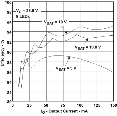
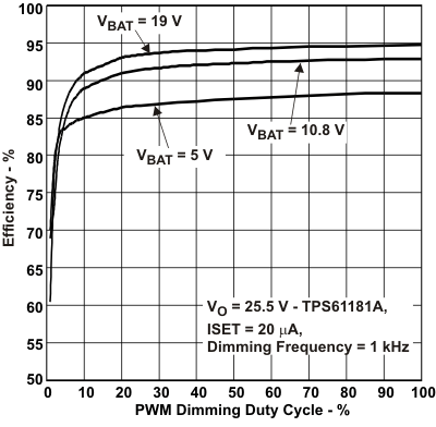
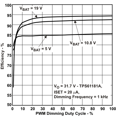
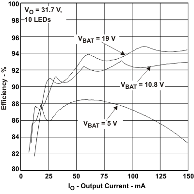
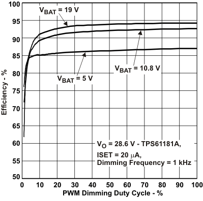
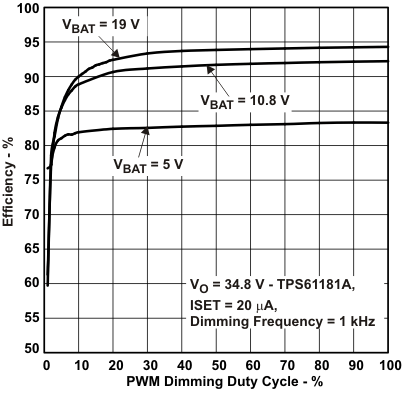
9.3 Additional Application Circuits
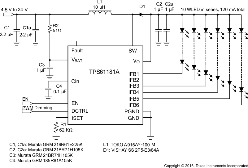 Figure 16. Audible Noise-Reduction Circuit
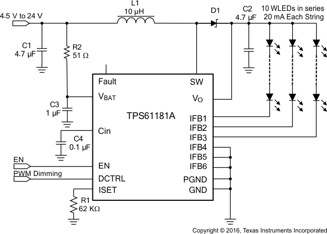 Figure 17. TPS61181A for Three Strings of LEDs
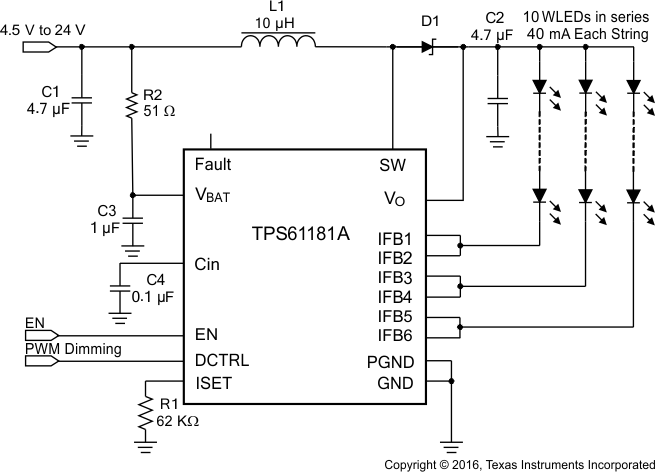 Figure 18. TPS61181A for Three Strings of LEDs With Double Current
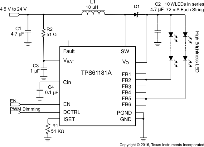 Figure 19. TPS61181A for Two Strings, High-Brightness LEDs Application
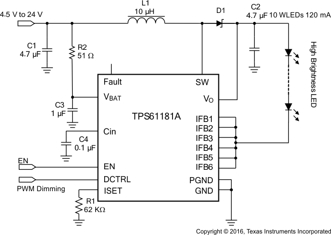 Figure 20. TPS61181A for One-String, High-Brightness LED Application
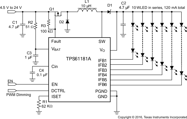 Figure 21. TPS61181A Driving External PFET for True Shutdown Application
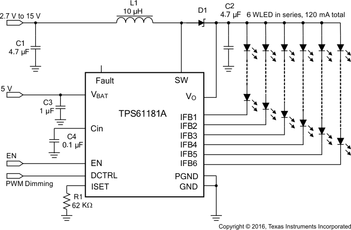 Figure 22. TPS61181A With Separate VBAT Power for Low Voltage-Input Application
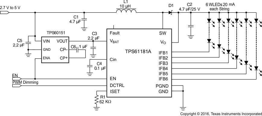 Figure 23. TPS61181A + TPS60151 for One Cell Li-Ion Battery Power Application