SLVSAW2C March 2012 – October 2016
PRODUCTION DATA.
- 1 Features
- 2 Applications
- 3 Description
- 4 Revision History
- 5 Device Comparison Table
- 6 Pin Configuration and Functions
- 7 Specifications
-
8 Detailed Description
- 8.1 Overview
- 8.2 Functional Block Diagram
- 8.3
Feature Description
- 8.3.1 Enable and Disable (EN)
- 8.3.2 Softstart (SS) and Hiccup Current Limit During Startup
- 8.3.3 Voltage Tracking (SS)
- 8.3.4 Short Circuit Protection (Hiccup-Mode)
- 8.3.5 Output Discharge Function
- 8.3.6 Power Good Output (PG)
- 8.3.7 Frequency Set Pin (FREQ)
- 8.3.8 Undervoltage Lockout (UVLO)
- 8.3.9 Thermal Shutdown
- 8.3.10 Charge Pump (CP, CN)
- 8.4 Device Functional Modes
- 9 Application and Implementation
- 10Power Supply Recommendations
- 11Layout
- 12Device and Documentation Support
- 13Mechanical, Packaging, and Orderable Information
11 Layout
11.1 Layout Guideline
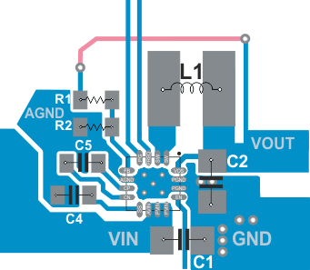
- It is recommended to place the input capacitor as close as possible to the IC pins PVIN and PGND.
- The VOS connection is noise sensitive and needs to be routed as short and directly to the output pin of the inductor.
- The exposed thermal pad of the package, analog ground (pin 6) and power ground (pin 14, 15) should have a single joint connection at the exposed thermal pad of the package. This minimizes switch node jitter.
- The charge pump capacitor connected to CP and CN should be placed close to the IC to minimize coupling of switching waveforms into other traces and circuits.
- Refer to Figure 29 and the evaluation module User Guide (SLVU670) for an example of component placement, routing and thermal design.
