SLVSCA0C October 2013 – September 2016
PRODUCTION DATA.
- 1 Features
- 2 Applications
- 3 Description
- 4 Revision History
- 5 Pin Configuration and Functions
- 6 Specifications
- 7 Detailed Description
- 8 Application and Implementation
- 9 Power Supply Recommendations
- 10Layout
- 11Device and Documentation Support
- 12Mechanical, Packaging, and Orderable Information
10 Layout
10.1 Layout Guidelines
10.1.1 Package Mounting
Solder-pad footprint recommendations for the TPS7B4250-Q1 device are available in the Mechanical, Packaging, and Orderable Information section and at www.ti.com.
10.1.2 Board Layout Recommendations to Improve PSRR and Noise Performance
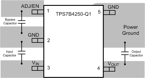
To improve AC performance such as PSRR, output noise, and transient response, TI recommends to design the board with separate ground planes for VIN and VOUT, with each ground plane connected only at the GND pin of the device. In addition, the ground connection for the output capacitor must connect directly to the GND pin of the device.
Equivalent series inductance (ESL) and ESR must be minimized in order to maximize performance and ensure stability. Every capacitor must be placed as close as possible to the device and on the same side of the PCB as the regulator.
Do not place any of the capacitors on the opposite side of the PCB from where the regulator is installed. The use of vias and long traces is strongly discouraged because of the negative impact on system performance. Vias and long traces can also cause instability.
If possible, and to ensure the maximum performance denoted in this product data sheet, use the same layout pattern used for TPS7B4250 evaluation board, available at www.ti.com.
10.2 Layout Example
 Figure 19. TPS7B4250-Q1 Layout Example
10.3 Power Dissipation and Thermal Considerations
Device power dissipation is calculated with Equation 1.

where
- PD = continuous power dissipation
- IO = output current
- VI = input voltage
- VO = output voltage
- IQ = quiescent current
As IQ « IO, the term IQ × VI in Equation 1 can be ignored.
For a device under operation at a given ambient air temperature (TA), calculate the junction temperature (TJ) with Equation 2.

where
- θJA = junction-to-junction-ambient air thermal impedance
A rise in junction temperature because of power dissipation can be calculated with Equation 3.

For a given maximum junction temperature (TJM), the maximum ambient air temperature (TAM) at which the device can operate can be calculated with Equation 4.
