9.2.3 Application Curves
VIN=5V, VOUT=1.8V, TA=25°C, BOM = Table 2, (unless otherwise noted)
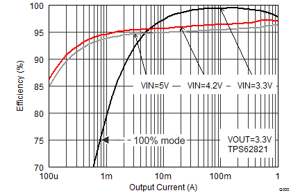 Figure 8. Efficiency TPS62821 at VOUT=3.3V
 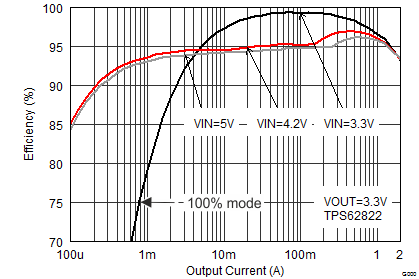 Figure 10. Efficiency TPS62822 at VOUT=3.3V
 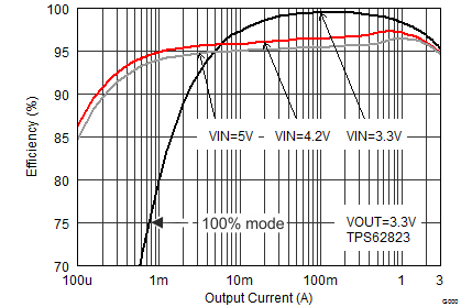 Figure 12. Efficiency TPS62823 at VOUT=3.3V
 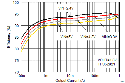 Figure 14. Efficiency TPS62821 at VOUT=1.8V
 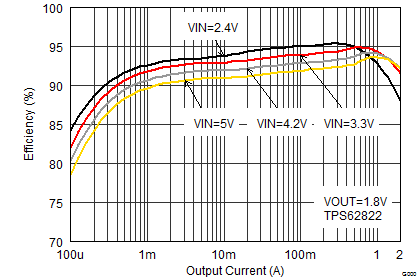 Figure 16. Efficiency TPS62822 at VOUT=1.8V
 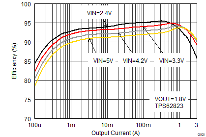 Figure 18. Efficiency TPS62823 at VOUT=1.8V
 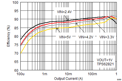 Figure 20. Efficiency TPS62821 at VOUT=1V
 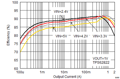 Figure 22. Efficiency TPS62822 at VOUT=1V
 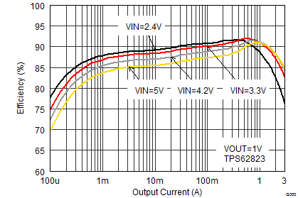 Figure 24. Efficiency TPS62823 at VOUT=1V
 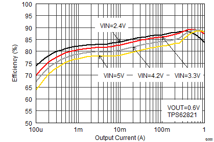 Figure 26. Efficiency TPS62821 at VOUT=0.6V
 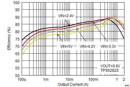 Figure 28. Efficiency TPS62822 at VOUT=0.6V
 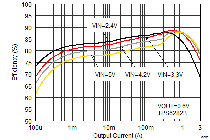 Figure 30. Efficiency TPS62823 at VOUT=0.6V
 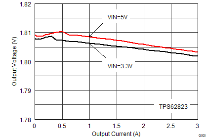 Figure 32. Output Voltage Accuracy (Load Regulation)
 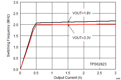 Figure 34. Switching Frequency vs Output Current
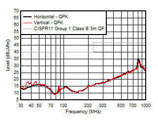
| RLOAD = 2.20 Ω, VIN = 5.5 V (battery supply), VOUT = 1.8 V, EMI test board without filters |
Figure 36. TPS62821 Radiated Emission 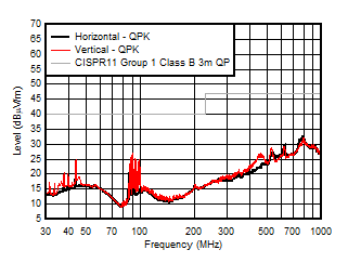
| RLOAD = 0.68 Ω, VIN = 5.5 V (battery supply), VOUT = 1.8 V, EMI test board without filters |
Figure 38. TPS62823 Radiated Emission 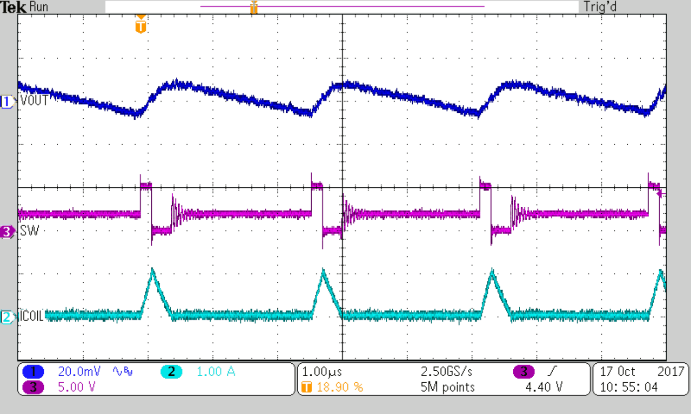 Figure 40. Typical Operation PSM
 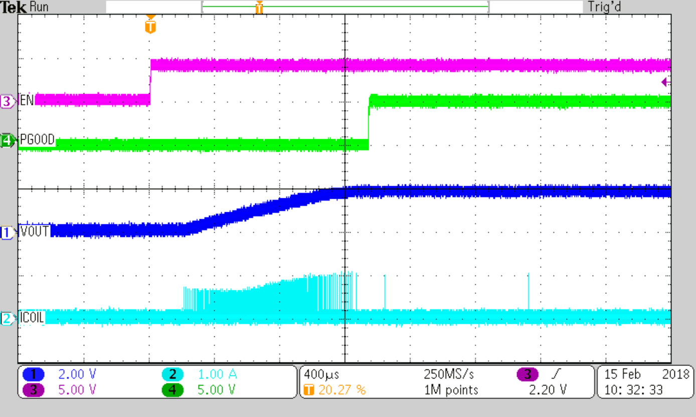 Figure 42. Startup at No Load
 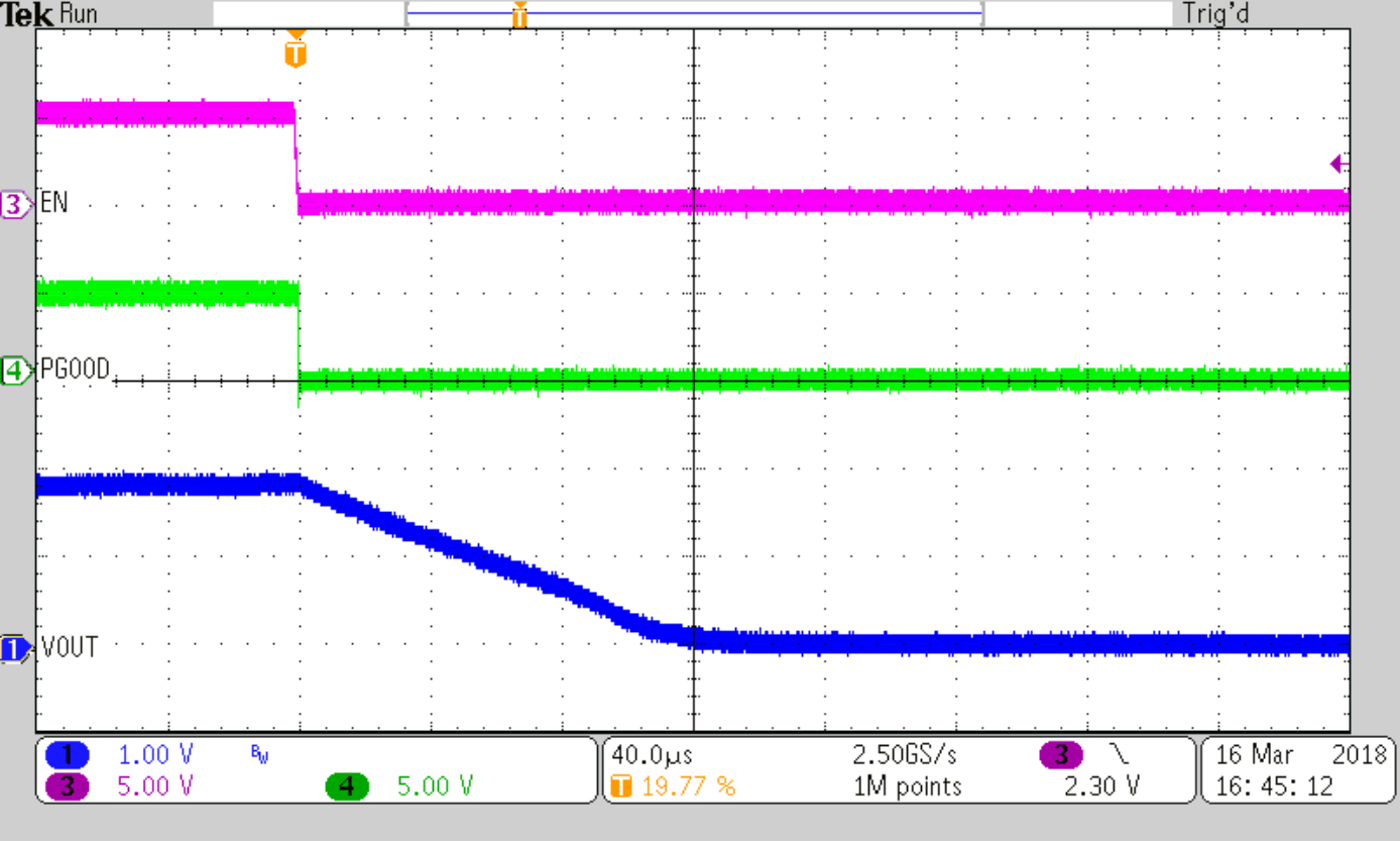 Figure 44. Active Output Discharge at No Load
 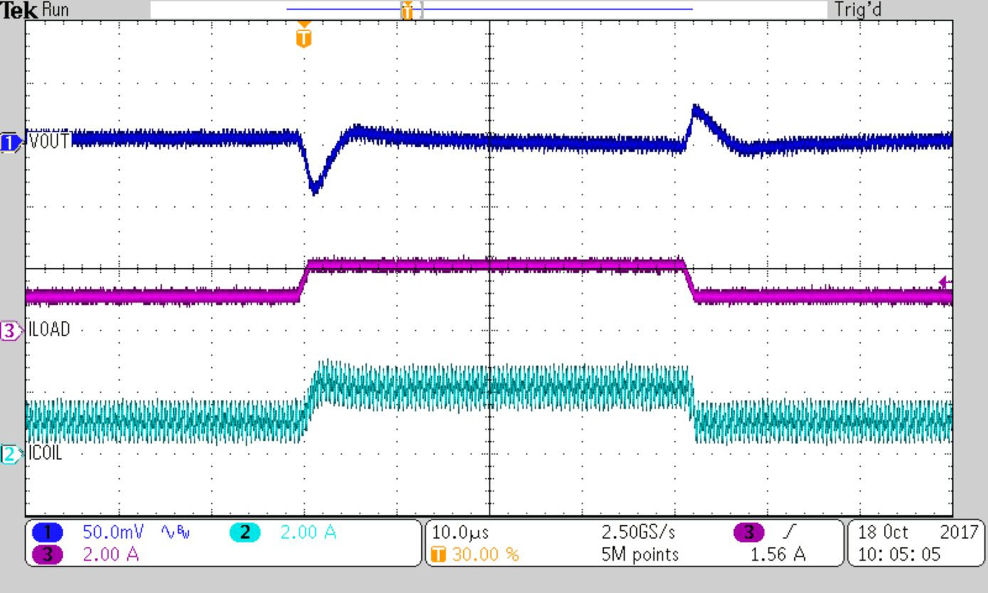 Figure 46. Load Transient Response, 1A to 2A, TPS62822
 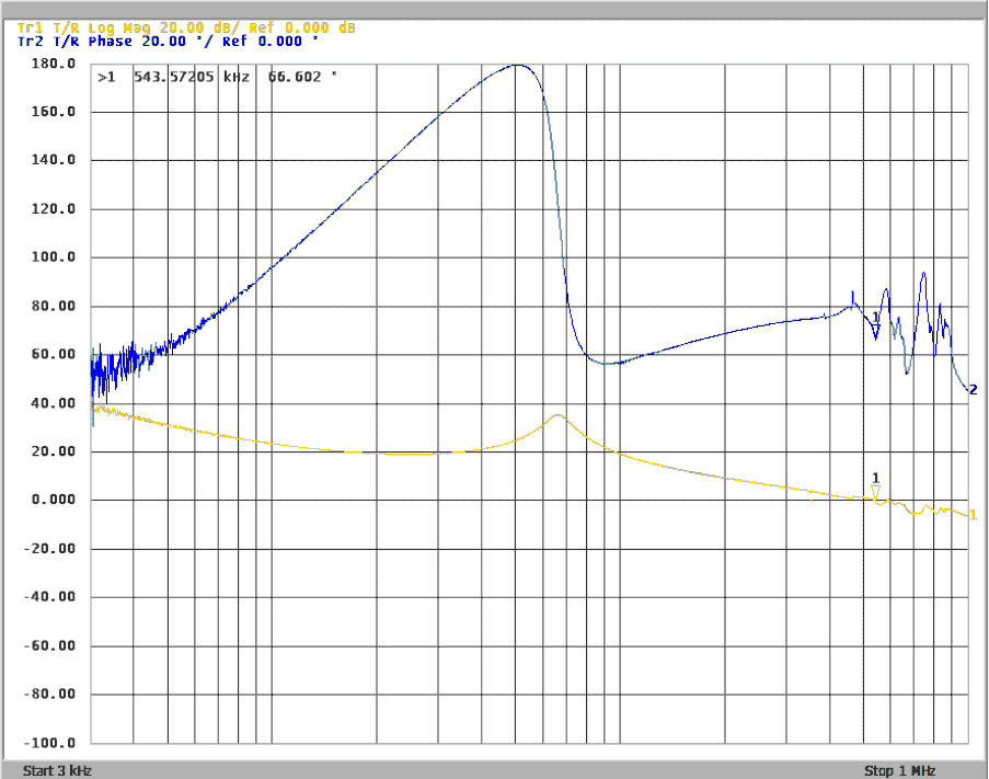 Figure 48. Frequency Response (TPS62823), IOUT=3A
 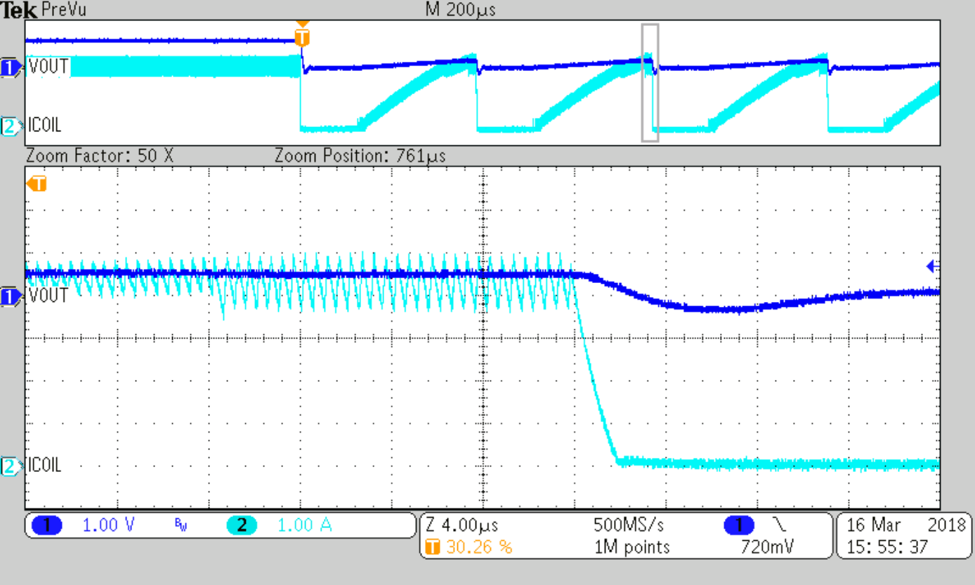 Figure 50. Overload Response of TPS62823 (Hiccup cycle)
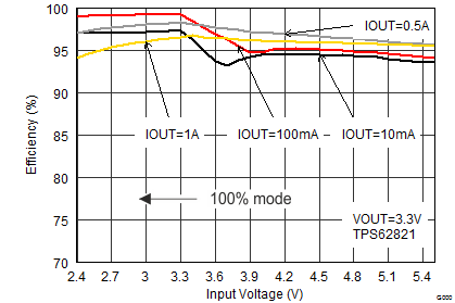 Figure 9. Efficiency TPS62821 at VOUT=3.3V
 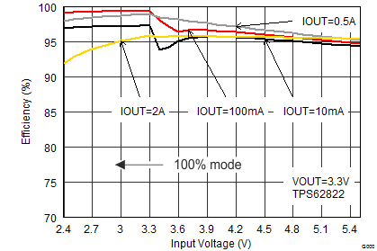 Figure 11. Efficiency TPS62822 at VOUT=3.3V
 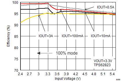 Figure 13. Efficiency TPS62823 at VOUT=3.3V
 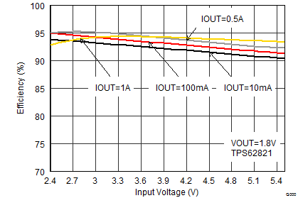 Figure 15. Efficiency TPS62821 at VOUT=1.8V
 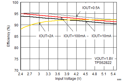 Figure 17. Efficiency TPS62822 at VOUT=1.8V
 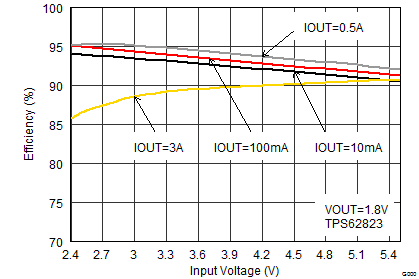 Figure 19. Efficiency TPS62823 at VOUT=1.8V
 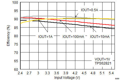 Figure 21. Efficiency TPS62821 at VOUT=1V
 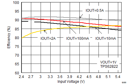 Figure 23. Efficiency TPS62822 at VOUT=1V
 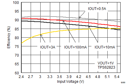 Figure 25. Efficiency TPS62823 at VOUT=1V
 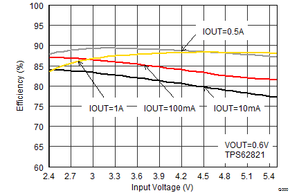 Figure 27. Efficiency TPS62821 at VOUT=0.6V
 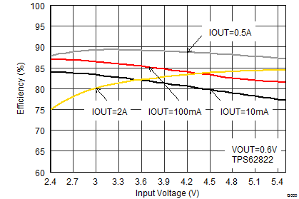 Figure 29. Efficiency TPS62822 at VOUT=0.6V
 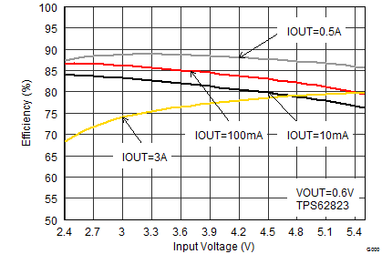 Figure 31. Efficiency TPS62823 at VOUT=0.6V
 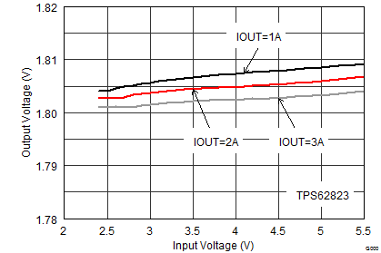 Figure 33. Output Voltage Accuracy (Line Regulation)
 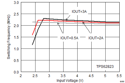 Figure 35. Switching Frequency vs Input Voltage
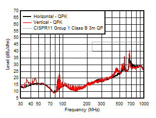
| RLOAD = 1.00 Ω, VIN = 5.5 V (battery supply), VOUT = 1.8 V, EMI test board without filters |
Figure 37. TPS62822 Radiated Emission 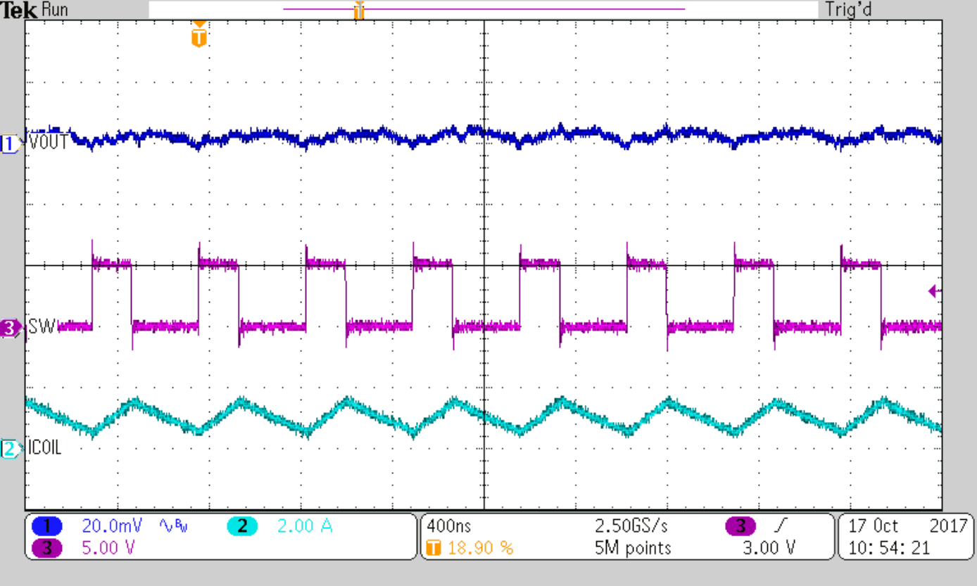 Figure 39. Typical Operation PWM
 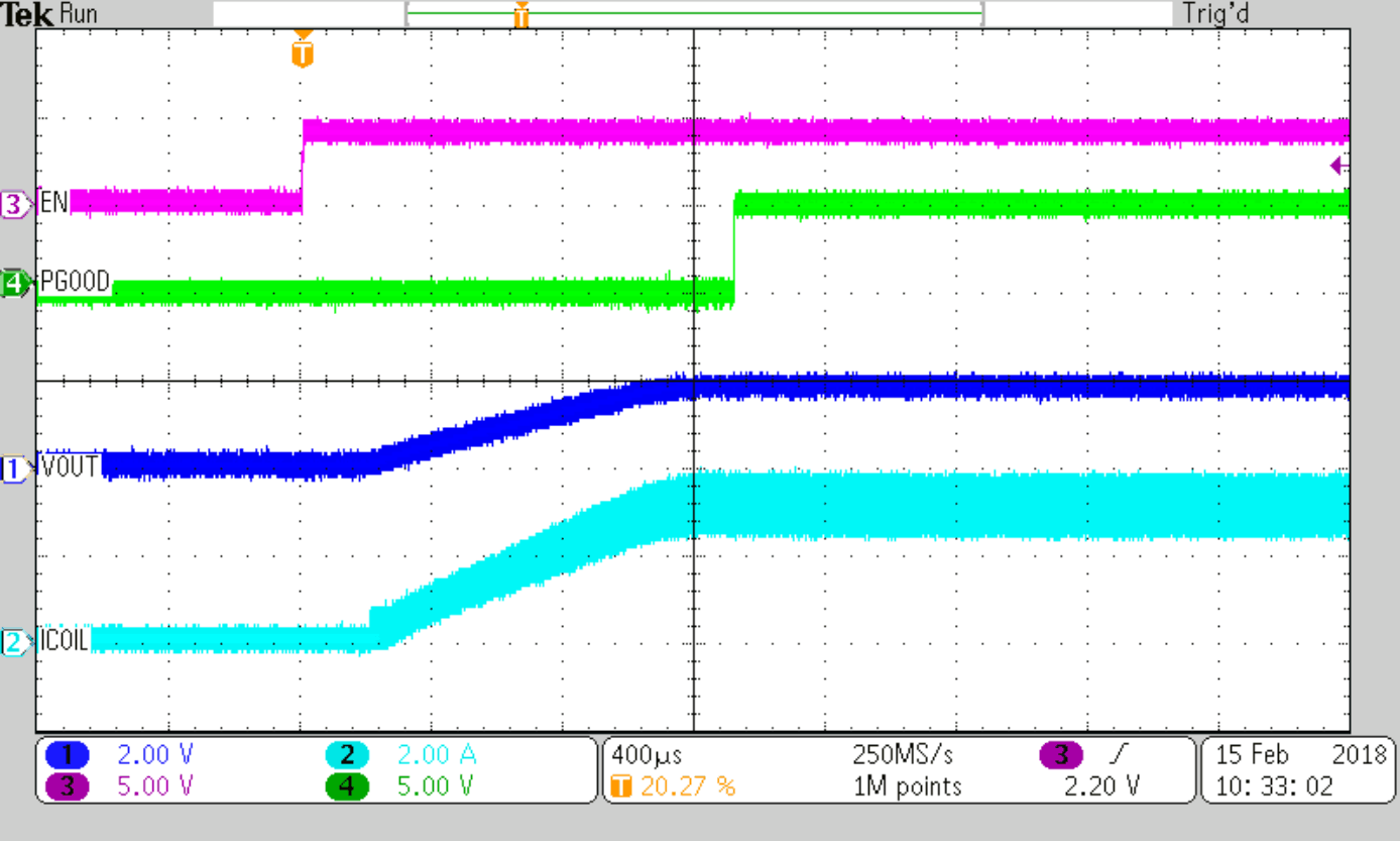 Figure 41. Startup into 0.6-Ohm (TPS62823)
 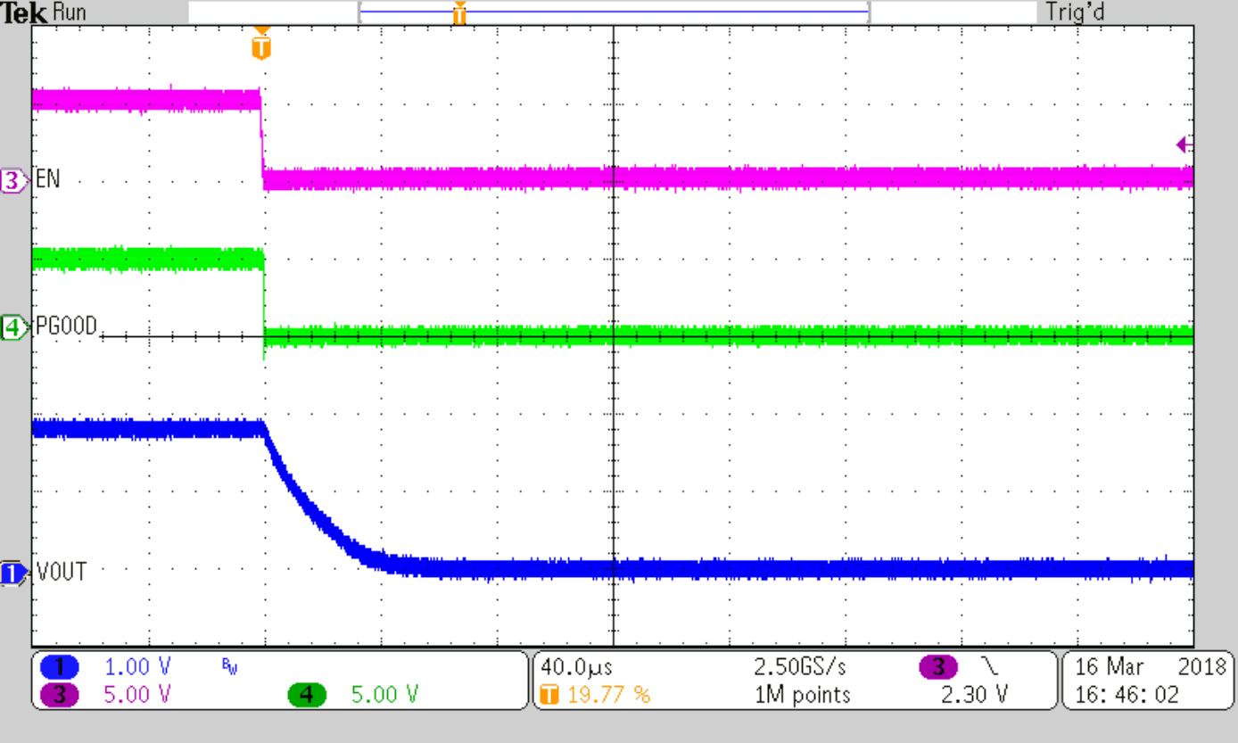 Figure 43. Active Output Discharge at load 1.8-Ohm
 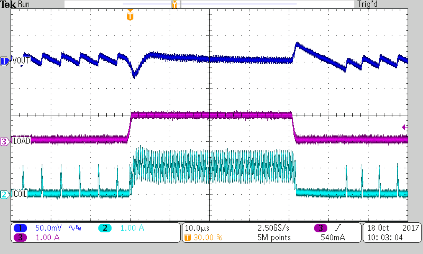 Figure 45. Load Transient Response, 50mA to 1A, TPS62822
 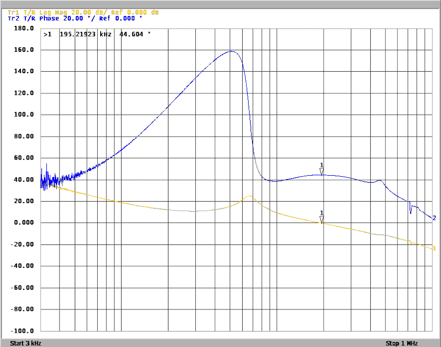 Figure 47. Frequency Response (TPS62823), IOUT=3A
 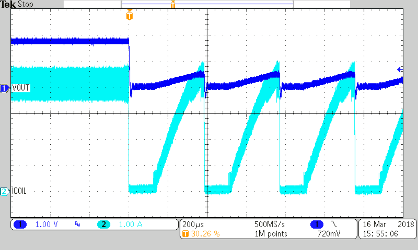 Figure 49. Overload Response of TPS62823
 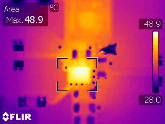 Figure 51. Device Temperature Rise on TPS62823 EVM at IOUT=3A


 Figure 50. Overload Response of TPS62823 (Hiccup cycle)


 Figure 49. Overload Response of TPS62823
  Figure 51. Device Temperature Rise on TPS62823 EVM at IOUT=3A