SLVSE94G September 2018 – June 2024
PRODUCTION DATA
- 1
- 1 Features
- 2 Applications
- 3 Description
- 4 Device Comparison Table
- 5 Pin Configuration and Functions
- 6 Specifications
- 7 Parameter Measurement Information
-
8 Detailed Description
- 8.1 Overview
- 8.2 Functional Block Diagram
- 8.3
Feature Description
- 8.3.1 Hot Plug-In and Inrush Current Control
- 8.3.2 PGOOD and PGTH
- 8.3.3 Undervoltage Lockout (UVLO)
- 8.3.4 Overvoltage Protection (OVP)
- 8.3.5 Input Reverse Polarity Protection (B_GATE, DRV)
- 8.3.6 Reverse Current Protection
- 8.3.7 Overload and Short-Circuit Protection
- 8.3.8 Output Power Limiting, PLIM (TPS26632, TPS26633, TPS26635, TPS26636, and TPS26637 Only)
- 8.3.9 Current Monitoring Output (IMON)
- 8.3.10 FAULT Response (FLT)
- 8.3.11 IN_SYS, IN, OUT, and GND Pins
- 8.3.12 Thermal Shutdown
- 8.3.13 Low Current Shutdown Control (SHDN)
- 8.4 Device Functional Modes
-
9 Application and Implementation
- 9.1 Application Information
- 9.2
Typical Application: Power Path Protection in a PLC System
- 9.2.1 Design Requirements
- 9.2.2 Detailed Design Procedure
- 9.2.3 Application Curves
- 9.3 System Examples
- 9.4 Dos and Do Nots
- 9.5 Power Supply Recommendations
- 9.6 Layout
- 10Device and Documentation Support
- 11Revision History
- 12Mechanical, Packaging, and Orderable Information
8.3.7.2.1 Start-Up With Short Circuit on Output
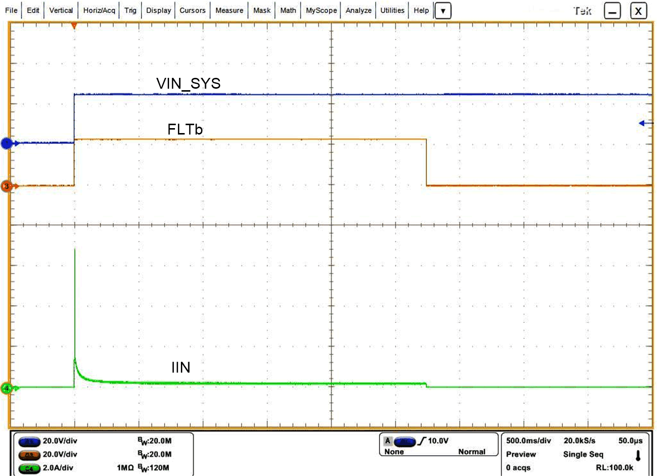
When the device is started with short circuit on the output, the current begins to limit at I(OL). Due to high power dissipation of VIN × I(OL) within the device the junction temperature increases. Subsequently, the thermal regulation control loop limits the load current to regulate the junction temperature at T(J_REG), 145°C (typical) for a duration of t(Treg_timeout), 2.5 seconds (typical). Subsequent operation of the device depends on the MODE configuration (auto-retry or latch-off) setting as per the Table 8-1. FLT gets asserted after t(Treg_timeout) and remains asserted till the output short circuit is removed. Figure 8-17 illustrates the behavior of the device in this condition.

| VIN = 24 V | RILIM = 3 kΩ |