SLVSEX0A March   2019  – July 2019

PRODUCTION DATA.  

  1. Features
  2. Applications
  3. Description
    1.     Device Images
      1.      Simplified Schematic
  4. Revision History
  5. Pin Configuration and Functions
    1.     Pin Functions
  6. Specifications
    1. 6.1 Absolute Maximum Ratings
    2. 6.2 ESD Ratings
    3. 6.3 Recommended Operating Conditions
    4. 6.4 Thermal Information
    5. 6.5 Electrical Characteristics
    6. 6.6 Typical Characteristics
  7. Detailed Description
    1. 7.1 Overview
    2. 7.2 Functional Block Diagram
    3. 7.3 Feature Description
      1. 7.3.1 Undervoltage Lockout
      2. 7.3.2 Enable and Disable
      3. 7.3.3 Soft Start
      4. 7.3.4 Frequency Select (FREQ)
    4. 7.4 Device Functional Modes
      1. 7.4.1 PWM Mode
      2. 7.4.2 PFM Mode
  8. Application and Implementation
    1. 8.1 Application Information
    2. 8.2 Typical Applications
      1. 8.2.1 12-V Output Boost Converter With External Bias
        1. 8.2.1.1 Design Requirements
        2. 8.2.1.2 Detailed Design Procedure
          1. 8.2.1.2.1 Programming the Output Voltage
          2. 8.2.1.2.2 Inductor Selection
          3. 8.2.1.2.3 Input and Output Capacitor Selection
          4. 8.2.1.2.4 Diode Rectifier Selection
        3. 8.2.1.3 Application Curves
      2. 8.2.2 14-V Output Boost Converter
        1. 8.2.2.1 Design Requirements
        2. 8.2.2.2 Detailed Design Procedure
          1. 8.2.2.2.1 Inductor Selection
          2. 8.2.2.2.2 Input and Output Capacitor Selection
  9. Power Supply Recommendations
  10. 10Layout
    1. 10.1 Layout Guidelines
    2. 10.2 Layout Example
  11. 11Device and Documentation Support
    1. 11.1 Device Support
      1. 11.1.1 Third-Party Products Disclaimer
    2. 11.2 Receiving Notification of Documentation Updates
    3. 11.3 Community Resources
    4. 11.4 Trademarks
    5. 11.5 Electrostatic Discharge Caution
    6. 11.6 Glossary
  12. 12Mechanical, Packaging, and Orderable Information

14-V Output Boost Converter

In this design example, TLV61048 is configured to output 14-V DC voltage. 1-MHz switching frequency is selected to reduce output ripple. TI recommends placing an RC snubber from the switch node to the ground node to ensure voltage spike does not exceed the specified absolute maximum rating.
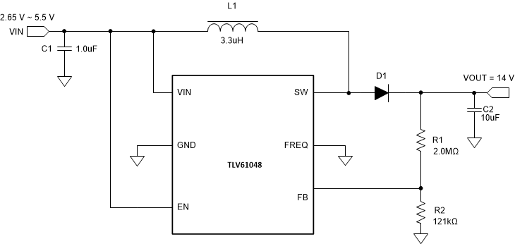
TLV61048 14V-App-Schematic_SLVSEX0.gifFigure 14. 14-V Boost Converter