SLVU097B October   2003  – October 2021 TPS54350


  1.   Trademarks
  2. 1Introduction
    1. 1.1 Background
    2. 1.2 Performance Specification Summary
    3. 1.3 Modifications
      1. 1.3.1 Output Voltage Setpoint
      2. 1.3.2 Switching Frequency
      3. 1.3.3 Input Filter
      4. 1.3.4 UVLO Programming
      5. 1.3.5 Synchronization
      6. 1.3.6 Power Good
      7. 1.3.7 Synchronous Low-Side FET
      8. 1.3.8 Optional Output Filtering
  3. 2Test Setup and Results
    1. 2.1  Input/Output Connections
    2. 2.2  Efficiency
    3. 2.3  Power Dissipation
    4. 2.4  Output Voltage Regulation
    5. 2.5  Load Transients
    6. 2.6  Loop Characteristic
    7. 2.7  Output Voltage Ripple
    8. 2.8  Input Voltage Ripple
    9. 2.9  Gate Drive
    10. 2.10 Powering Up and Down
  4. 3Board Layout
    1. 3.1 Layout
  5. 4Schematic and Bill of Materials
    1. 4.1 Bill of Materials
  6. 5Revision History

Loop Characteristic

The TPS54350EVM−235 loop response characteristics are shown in Figure 2-7 and Figure 2-8. Gain and phase plots are shown for each device at minimum and maximum operating voltage.
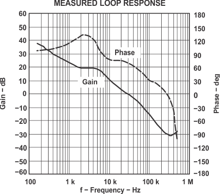
GUID-20210929-SS0I-BTRT-6XCF-RNWPF0CNP5TL-low.gif Figure 2-7 Measured Loop Response, TPS54350, VI = 6 V
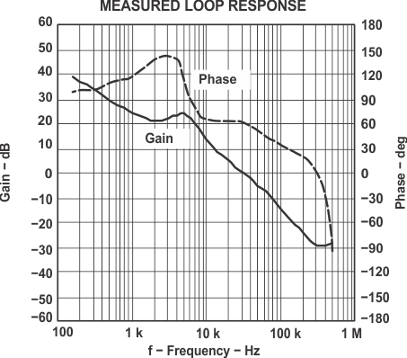
GUID-20210929-SS0I-9WJV-HMLM-7KWHCZJBH0FD-low.gif Figure 2-8 Measured Loop Response, TPS54350, VI = 18 V