SLVU151A April   2013  – August 2021 TPS54350 , TPS54550


  1.   Trademarks
  2. 1Background
  3. 2Performance Specification Summary
  4. 3Modifications
    1. 3.1 Output Voltage Set Point
    2. 3.2 Input Voltage Range
  5. 4Test Setup and Results
    1. 4.1 Input / Output Connections
    2. 4.2 Efficiency
    3. 4.3 Output Voltage Regulation
    4. 4.4 Load Transients
    5. 4.5 Loop Characteristics
    6. 4.6 Output Voltage Ripple
    7. 4.7 Input Voltage Ripple
    8. 4.8 Powering Up
  6. 5Board Layout
    1. 5.1 Layout
  7. 6Schematic and Bill of Materials
    1. 6.1 Schematic
    2. 6.2 Bill of Materials
  8. 7Revision History

Input Voltage Ripple

The input voltage ripple is shown in Figure 4-7. The input voltage is VIN = 12 V for the TPS54550. Output current for each device is at full rate TPS54550EVM-158 load of 5 A.
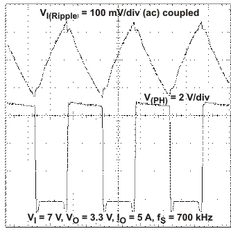
GUID-1A27F25B-C3CF-4177-BB01-9A4019A52288-low.gifFigure 4-7 Input Voltage Ripple, TPS54550