SLVU157A March   2006  – October 2021 TPS5430 , TPS5431


  1.   Trademarks
  2. 1Introduction
    1. 1.1 Background
    2. 1.2 Performance Specification Summary
    3. 1.3 Modifications
      1. 1.3.1 Output Voltage Set Point
  3. 2Test Setup and Results
    1. 2.1 Input/Output Connections
    2. 2.2 Efficiency
    3. 2.3 Output Voltage Load Regulation
    4. 2.4 Output voltage Line Regulation
    5. 2.5 Load Transients
    6. 2.6 Loop Characteristics
    7. 2.7 Output Voltage Ripple
    8. 2.8 Input Voltage Ripple
    9. 2.9 Powering Up
  4. 3Board Layout
    1. 3.1 Layout
  5. 4Schematic and Bill of Materials
    1. 4.1 Schematic
    2. 4.2 Bill of Materials
  6. 5Revision History

Input Voltage Ripple

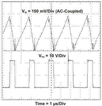
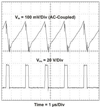
The TPS5430EVM-173 and TPS5431EVM-173 input voltage ripple is shown in Figure 2-13 and Figure 2-14. The output current for each device is at full rated load of 3 A.
GUID-1A223905-3FBE-4001-8E23-DCBBD1F367C0-low.gifFigure 2-13 TPS5430 Input Ripple
GUID-DFECF222-D9A3-44E5-8DEA-6A4A388B4C21-low.gifFigure 2-14 TPS5431 Input Ripple