SLVU263A August   2008  – October 2021 TPS54231


  1.   Trademarks
  2. 1Introduction
    1. 1.1 Background
    2. 1.2 Performance Specification Summary
    3. 1.3 Modifications
      1. 1.3.1 Output Voltage Set Point
  3. 2Test Setup and Results
    1. 2.1  Input / Output Connections
    2. 2.2  Efficiency
    3. 2.3  Output Voltage Load Regulation
    4. 2.4  Output Voltage Line Regulation
    5. 2.5  Load Transients
    6. 2.6  Loop Characteristics
    7. 2.7  Output Voltage Ripple
    8. 2.8  Input Voltage Ripple
    9. 2.9  Powering Up
    10. 2.10 Eco-mode Operation
    11. 2.11 Thermal Characteristics
  4. 3Board Layout
    1. 3.1 Layout
    2. 3.2 Estimated Circuit Area
  5. 4Schematic and Bill of Materials
    1. 4.1 Schematic
    2. 4.2 Bill of Materials
  6. 5Revision History

Input Voltage Ripple

The TPS54231EVM-372 input voltage ripple is shown in Figure 2-8 . The output current is the rated full load of 2 A and VIN = 15 V. The ripple voltage is measured directly across the input capacitors.
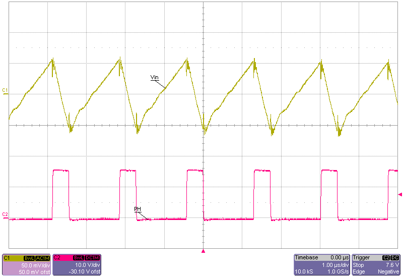
GUID-959C7CA4-ED5A-4656-A920-B3F560FABE33-low.png Figure 2-8 TPS54231EVM-372 Input Ripple