SLVU264A November   2008  – October 2021 TPS54233


  1.   Trademarks
  2. 1Introduction
    1. 1.1 Background
    2. 1.2 Performance Specification Summary
    3. 1.3 Modifications
      1. 1.3.1 Output Voltage Set Point
  3. 2Test Setup and Results
    1. 2.1 Input / Output Connections
    2. 2.2 Efficiency
    3. 2.3 Output Voltage Load Regulation
    4. 2.4 Output Voltage Line Regulation
    5. 2.5 Load Transients
    6. 2.6 Loop Characteristics
    7. 2.7 Output Voltage Ripple
    8. 2.8 Input Voltage Ripple
    9. 2.9 Powering Up
  4. 3Board Layout
    1. 3.1 Layout
    2. 3.2 Estimated Circuit Area
  5. 4Schematic and Bill of Materials
    1. 4.1 Schematic
    2. 4.2 Bill of Materials
  6. 5Revision History

Output Voltage Line Regulation

The line regulation for the TPS54233EVM-373 is shown in Figure 2-4.
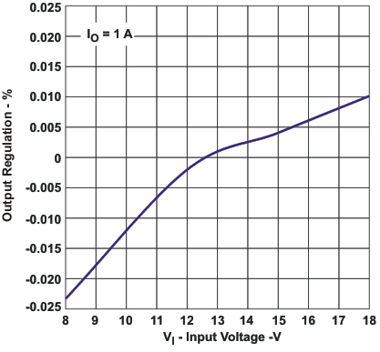
GUID-32739D43-51C5-424F-9A1F-D7574516FB9B-low.gif Figure 2-4 TPS54233EVM-373 Line Regulation