SLVU281B May   2009  – August 2021 TPS54620


  1.   Trademarks
  2. 1Introduction
    1. 1.1 Background
    2. 1.2 Performance Specification Summary
    3. 1.3 Modifications
      1. 1.3.1 Output Voltage Set Point
      2. 1.3.2 Slow Start Time
      3. 1.3.3 Track In
      4. 1.3.4 Adjustable UVLO
      5. 1.3.5 Input Voltage Rails
  3. 2Test Setup and Results
    1. 2.1  Input / Output Connections
    2. 2.2  Efficiency
    3. 2.3  Output Voltage Load Regulation
    4. 2.4  Output Voltage Line Regulation
    5. 2.5  Load Transients
    6. 2.6  Loop Characteristics
    7. 2.7  Output Voltage Ripple
    8. 2.8  Input Voltage Ripple
    9. 2.9  Powering Up
    10. 2.10 Thermal Characteristics
  4. 3Board Layout
    1. 3.1 Layout
    2. 3.2 Estimated Circuit Area
  5. 4Schematic and Bill of Materials
    1. 4.1 Schematic
    2. 4.2 Bill of Materials
  6. 5Revision History

Efficiency

The efficiency of this EVM peaks at a load current of about 2 A and then decreases as the load current increases towards full load. Figure 2-1 shows the efficiency for the TPS54620EVM-374 at an ambient temperature of 25°C.
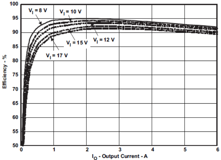
GUID-95B16DCC-F86D-4791-B4A7-0E1BF827A452-low.gifFigure 2-1 TPS54620EVM-374 Efficiency

Figure 2-2 shows the efficiency for the TPS54620EVM-374 at lower output currents below 0.10 A at an ambient temperature of 25°C.
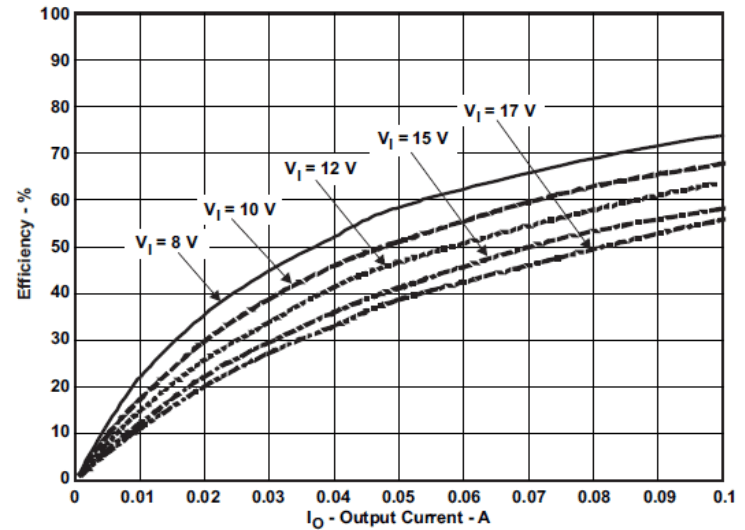
GUID-2E94B454-1A3A-4ACF-AAFF-00DD138157BA-low.gifFigure 2-2 TPS54620EVM-374 Low Current Efficiency

The efficiency may be lower at higher ambient temperatures, due to temperature variation in the drain-to-source resistance of the internal MOSFET.