SLVU379A August 2010 – August 2021 TPS54521
3.1 Layout
The board layout for the TPS54521EVM-607 is shown in Figure 3-1 through Figure 3-5. The topside layer of the EVM is laid out in a manner typical of a user application. The top, bottom and internal layers are 2-oz. copper.
The top layer contains the main power traces for PVIN, VIN, VOUT, and VPHASE. Also on the top layer are connections for the remaining pins of the TPS54521 and a large area filled with ground. The bottom and internal ground layers contain ground planes only. The top side ground traces are connected to the bottom and internal ground planes with multiple vias placed around the board including two vias directly under the TPS54521 device to provide a thermal path from the top-side ground plane to the bottom-side ground plane.
The input decoupling capacitors (C2, and C3) and bootstrap capacitor (C5) are all located as close to the IC as possible. In addition, the voltage set-point resistor divider components are also kept close to the IC. The voltage divider network ties to the output voltage at the point of regulation, the copper VOUT trace at the J3 output connector. For the TPS54521, an additional input bulk capacitor may be required, depending on the EVM connection to the input supply. Critical analog circuits such as the voltage setpoint divider, frequency set resistor, slow start capacitor and compensation components are terminated to ground using a wide ground trace separate from the power ground pour.
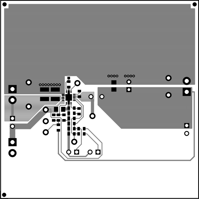 Figure 3-1 TPS54521EVM-607 Top-Side Layout (Top View)
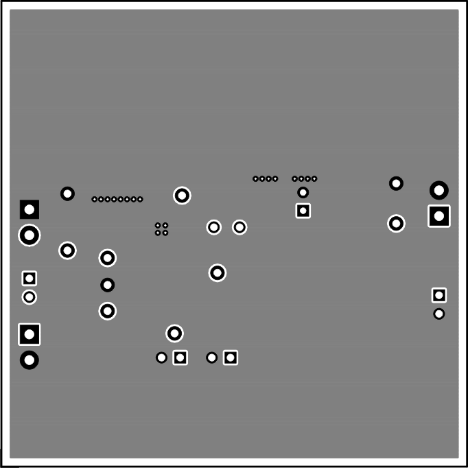 Figure 3-3 TPS54521EVM-607 Layer 3 (X-Ray Top View)
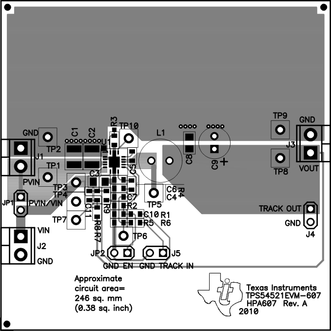 Figure 3-5 TPS54521EVM-607 Top-Side Assembly
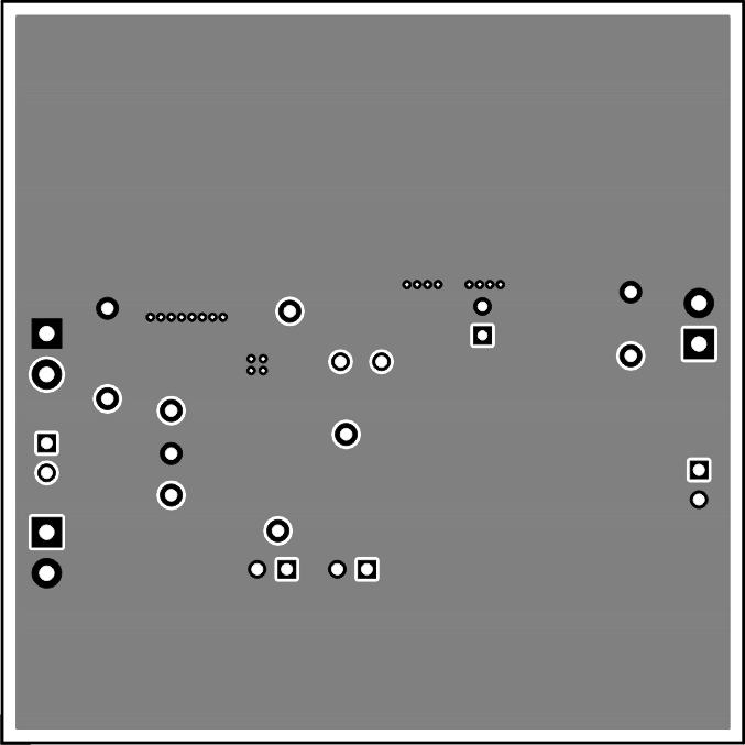 Figure 3-2 TPS54521EVM-607 Layer 2 (X-Ray Top View)
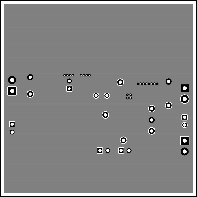 Figure 3-4 TPS54521EVM-607 Bottom-Side Layout (Bottom View)