SLVU411A September 2010 – June 2021 TPS62120
5.5 Typical Operation, 10 mA
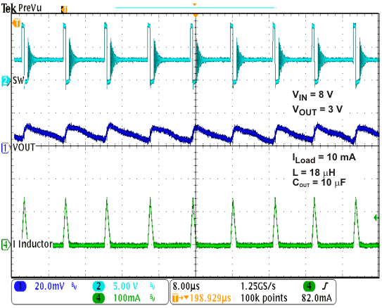
Figure 5-8 illustrates the typical output voltage ripple for the TPS62120 with a 10-mA load.
 Figure 5-8 TPS62120EVM Output Ripple, 10-mA Load(VIN = 8.0 V, VOUT = 3.0 V)
SLVU411A September 2010 – June 2021 TPS62120
Figure 5-8 illustrates the typical output voltage ripple for the TPS62120 with a 10-mA load.
 Figure 5-8 TPS62120EVM Output Ripple, 10-mA Load(VIN = 8.0 V, VOUT = 3.0 V)