SLVU411A September   2010  – June 2021 TPS62120


  1.   Trademarks
  2. 1Introduction
    1. 1.1 Features
    2. 1.2 Applications
  3. 2TPS62120EVM Schematic
  4. 3Connector and Test Point Descriptions
    1. 3.1 Enable Jumpers/Switches (RefDes) TPS62120
      1. 3.1.1  J1 VIN
      2. 3.1.2  J2 S+/S–
      3. 3.1.3  J3 GND
      4. 3.1.4  J4 VOUT
      5. 3.1.5  J5 S+/S–
      6. 3.1.6  J6 GND
      7. 3.1.7  JP1 EN
      8. 3.1.8  JP2 SGND
      9. 3.1.9  J7 VOUT (SMA)
      10. 3.1.10 J8 PG/GND
  5. 4Test Configuration
    1. 4.1 Hardware Setup
    2. 4.2 Procedure
  6. 5TPS62120EVM Test Data
    1. 5.1 Efficiency
    2. 5.2 Start-Up
    3. 5.3 Load Transient Response
    4. 5.4 Typical Operation, 60 mA
    5. 5.5 Typical Operation, 10 mA
    6. 5.6 Current Limit Operation
  7. 6TPS62120EVM Assembly Drawings and Layout
  8. 7Bill of Materials
  9. 8Revision History

TPS62120EVM Assembly Drawings and Layout

Figure 6-1 through Figure 6-3 show the design of the show the design of the TPS62120EVM-640 printed circuit board. The EVM has been designed using a four-layer, 1-ounce copper-clad PCB.

Note:

Board layouts are not to scale. These figures are intended to show how the board is laid out; they are not intended to be used for manufacturing TPS62120EVM-640 PCBs.
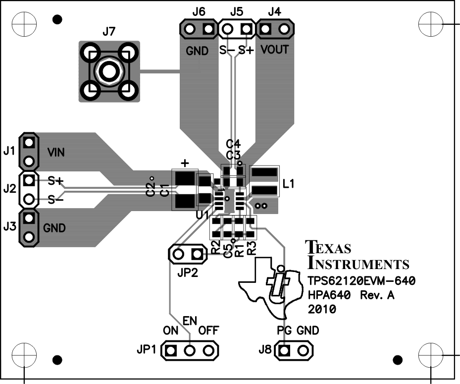
GUID-422F6EFF-0134-4731-9197-B35C836FDEDF-low.gifFigure 6-1 TPS62120EVM Component Placement (Top View)
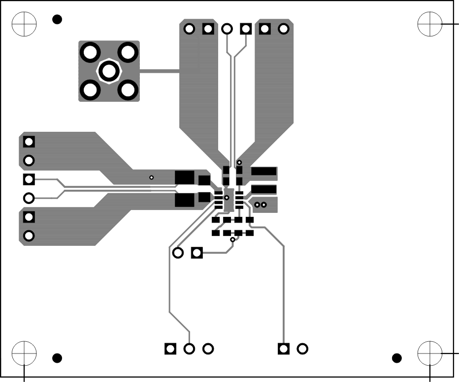
GUID-F24EDBB8-90E7-4D81-B16F-2E22EBBA2D6F-low.gifFigure 6-2 TPS62120EVM Top-Side Copper (Top View)
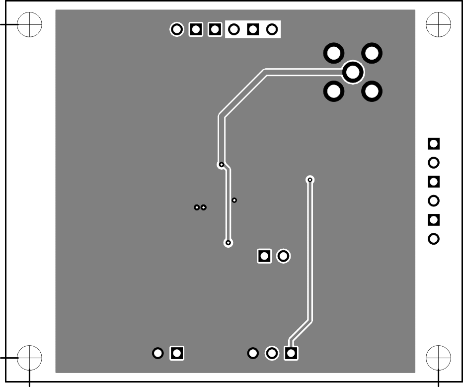
GUID-21B465F6-C579-45A8-968A-C235C4FC908F-low.gifFigure 6-3 TPS62120EVM Bottom-Side Copper (Bottom View)