SLVU642A May   2012  – August 2021 TPS54526


  1.   Trademarks
  2. 1Introduction
  3. 2Performance Specification Summary
  4. 3Modifications
    1. 3.1 Output Voltage Set Point
  5. 4Test Setup and Results
    1. 4.1  Input / Output Connections
    2. 4.2  Start-Up Procedure
    3. 4.3  Efficiency
    4. 4.4  Light-Load Efficiency
    5. 4.5  Load Regulation
    6. 4.6  Line Regulation
    7. 4.7  Load Transient Response
    8. 4.8  Output Voltage Ripple
    9. 4.9  Input Voltage Ripple
    10. 4.10 Start-Up
  6. 5Board Layout
    1. 5.1 Layout
  7. 6Schematic, Bill of Materials and Reference
    1. 6.1 Schematic
    2. 6.2 Bill of Materials
    3. 6.3 Reference
  8. 7Revision History

Schematic

Figure 6-1 is the schematic for the TPS54526EVM.
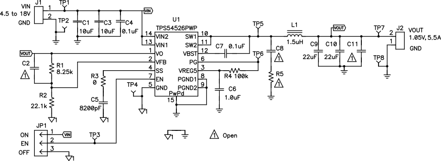
GUID-09613BD7-EC7E-4E51-9D89-600B716487B7-low.gifFigure 6-1 TPS54526EVM-608 Schematic Diagram