SLVU677A August 2012 – August 2021 TPS54494
- Trademarks
- 1Introduction
- 2Performance Specification Summary
- 3Modifications
- 4Test Setup and Results
- 5Board Layout
- 6Schematic, Bill of Materials, and Reference
- 7Revision History
5.1 Layout
The board layout for the TPS54494EVM is shown in Figure 5-1 through Figure 5-6. The top layer contains the main power traces for VIN and VOUTx. Also on the top layer are connections for the pins of the TPS54494 and a large area filled with ground. Many of the signal traces also are located on the top side. The input decoupling capacitors are located as close to the IC as possible. The input and output connectors, test points, and all of the assembled components are located on the top side. An analog ground (GND) area is provided on the top side. Analog ground (GND) and power ground (PGND) are connected at a single point on the top layer near the IC. The other layers are primarily power ground but the bottom layer has some traces to connect the test points for SSx and ENx.
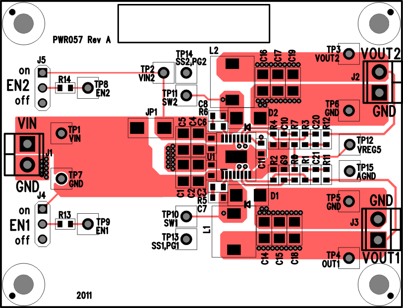 Figure 5-1 Top Assembly
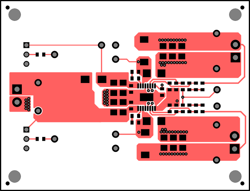 Figure 5-2 Top Layer
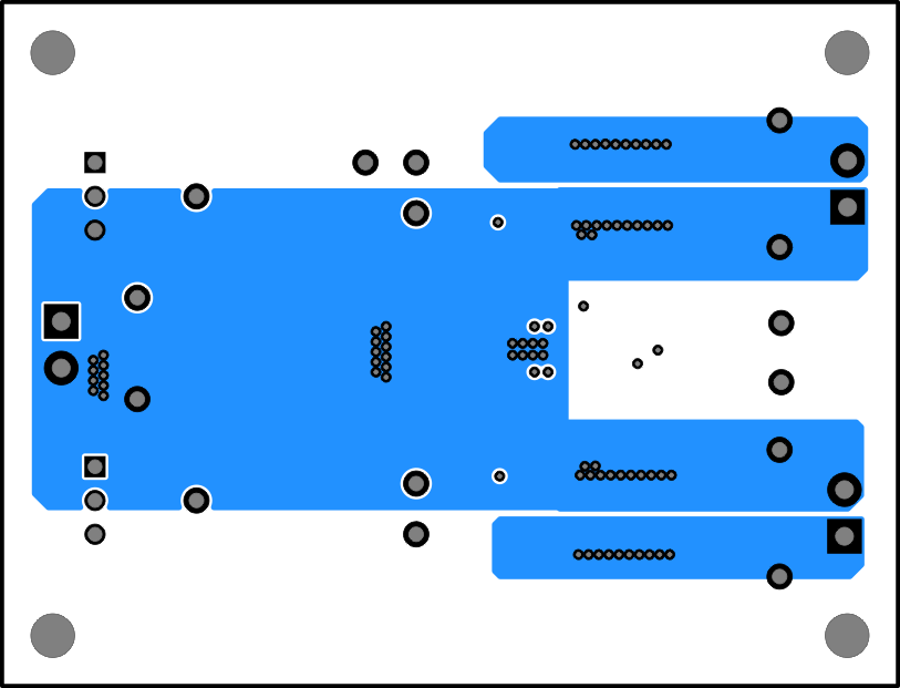 Figure 5-3 Internal 1 Layer
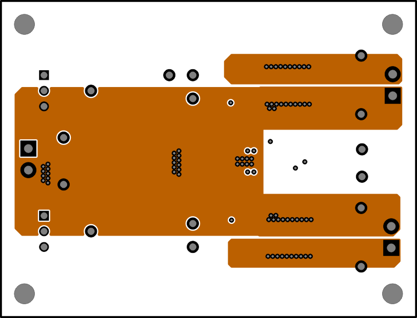 Figure 5-4 Internal 2 Layer
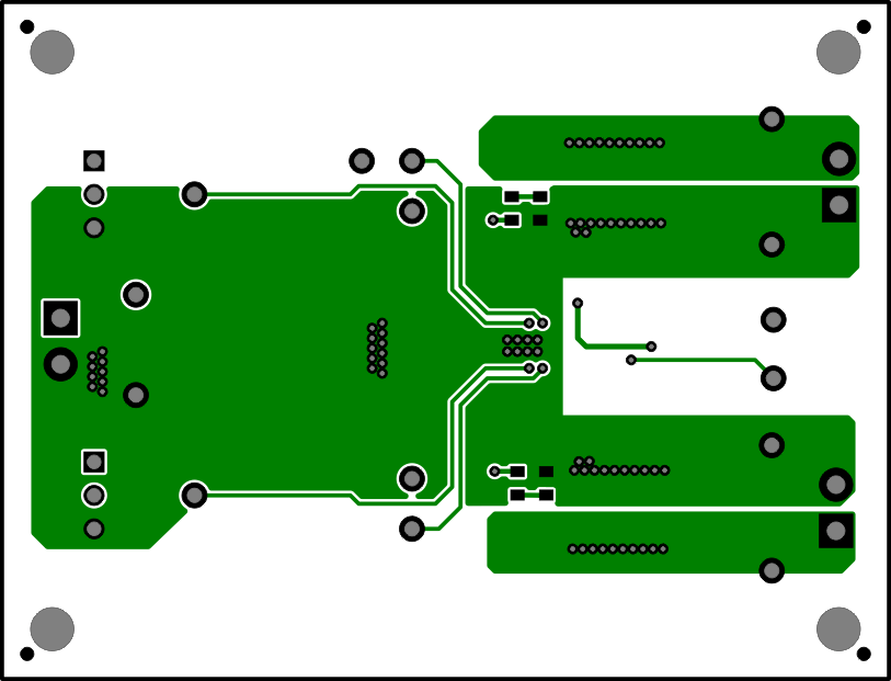 Figure 5-5 Bottom Layer
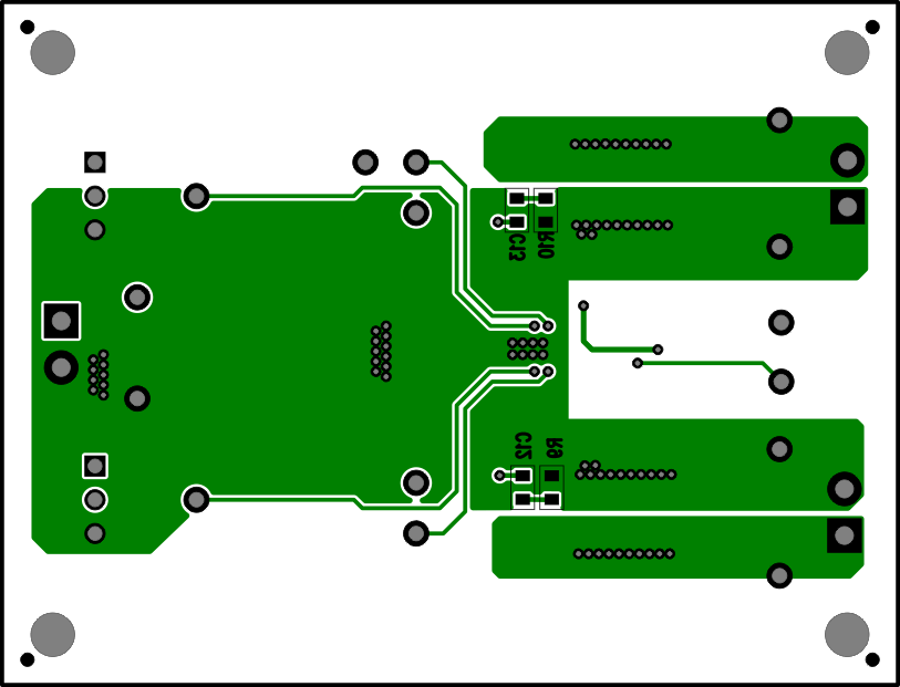 Figure 5-6 Bottom Assembly