SLVU745A August   2012  – May 2021 TPS54495


  1.   Trademarks
  2. 1Introduction
  3. 2Performance Specification Summary
  4. 3Modifications
    1. 3.1 Output Voltage Setpoint
    2. 3.2 Output Filter and Closed-Loop Response
  5. 4Test Setup and Results
    1. 4.1 Input/Output Connections
    2. 4.2 Start-Up Procedure
    3. 4.3 Efficiency
      1. 4.3.1 Efficiency of Converter 1
      2. 4.3.2 Efficiency of Converter 2
    4. 4.4 Load Regulation
      1. 4.4.1 Load Regulation of Converter 1
      2. 4.4.2 Load Regulation of Converter 2
    5. 4.5 Line Regulation
      1. 4.5.1 Line Regulation Converter 1
      2. 4.5.2 Line Regulation Converter 2
    6. 4.6 Load Transient Response
      1. 4.6.1 Load Transient Response Converter 1
      2. 4.6.2 Load Transient Response Converter 2
    7. 4.7 Output Voltage Ripple
      1. 4.7.1 Output Voltage Ripple Converter 1
      2. 4.7.2 Output Voltage Ripple Converter 2
    8. 4.8 Input Voltage Ripple
    9. 4.9 Start-Up
      1. 4.9.1 Converter 1 Start-Up
      2. 4.9.2 Converter 2 Start-Up
  6. 5Board Layout
    1. 5.1 Layout
  7. 6Schematic, Bill of Materials, and Reference
    1. 6.1 Schematic
    2. 6.2 Bill of Materials
    3. 6.3 Reference
  8. 7Revision History

Input Voltage Ripple

The TPS54495EVM input voltage ripple is shown in Figure 4-15. The output currents are the rated full load currents of 4 A CH1 and 2 A CH2.
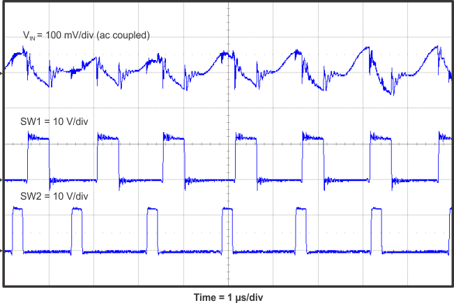
GUID-1ECD0206-1C8C-41FF-8828-A2ACDFBB6C7A-low.gifFigure 4-15 TPS54495EVM Input Voltage Ripple