SLVU777A September 2012 – November 2021 TPS54020
3.1 Layout
The board layout for the EVM is shown in Figure 3-1 through Figure 3-6. The top-side layer of the EVM is laid out in a manner typical of a user application. All 4 layers (top, bottom, and 2 internal) are 2-oz copper.
The top layer contains the main power traces for PVIN, VIN, VOUT and VPHASE. Also on the top layer are connections for several analog pins of the TPS54020 and a large area filled with PGND. The two internal layers are the same and contain mostly power planes, including PGND, VOUT, PVIN and VPHASE. The bottom layer contains the remainder of the analog circuit connections, plus power planes similar to the internal layers. The top-side power and ground planes are connected to the bottom and internal power and ground planes with multiple vias placed around the board including several vias directly under the TPS54020 device to provide a thermal path from the top-side power planes to the other layer power planes.
The input decoupling capacitor C4 and bootstrap capacitor C5 are both located as close to the IC as possible. Additionally, the voltage set-point resistor divider components are kept close to the IC. The location of the connection to the voltage divider network at R5 defines the point of regulation, which is the copper VOUT trace at the output connector J3. For the TPS54020, an additional input bulk capacitor is included to effectively reduce the source impedance from the input supply to the switcher. Critical analog circuits such as the voltage setpoint divider, frequency set resistor, slow-start capacitor, and compensation components are terminated to analog ground (AGND) using a ground trace that is separate from the power ground plane.
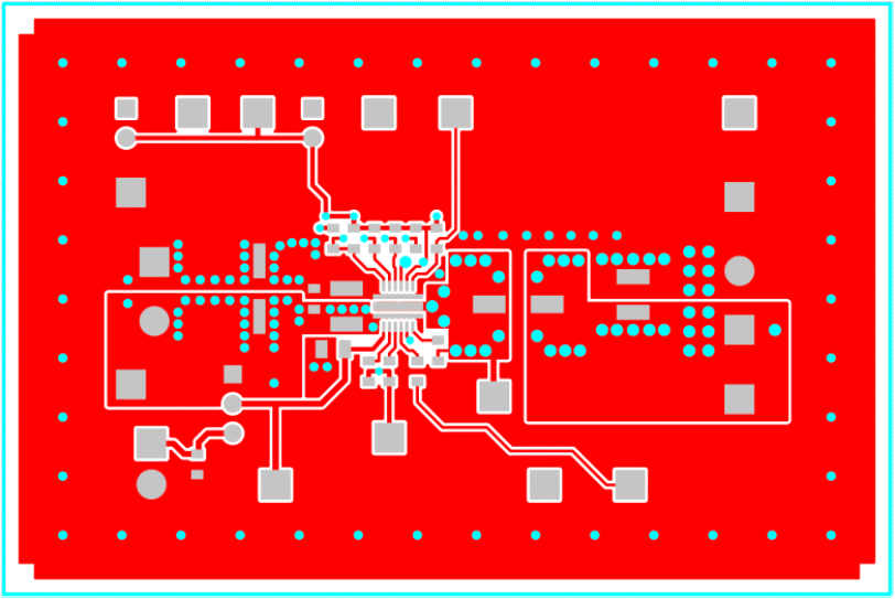 Figure 3-1 TPS54020EVM-082 Top Side Copper
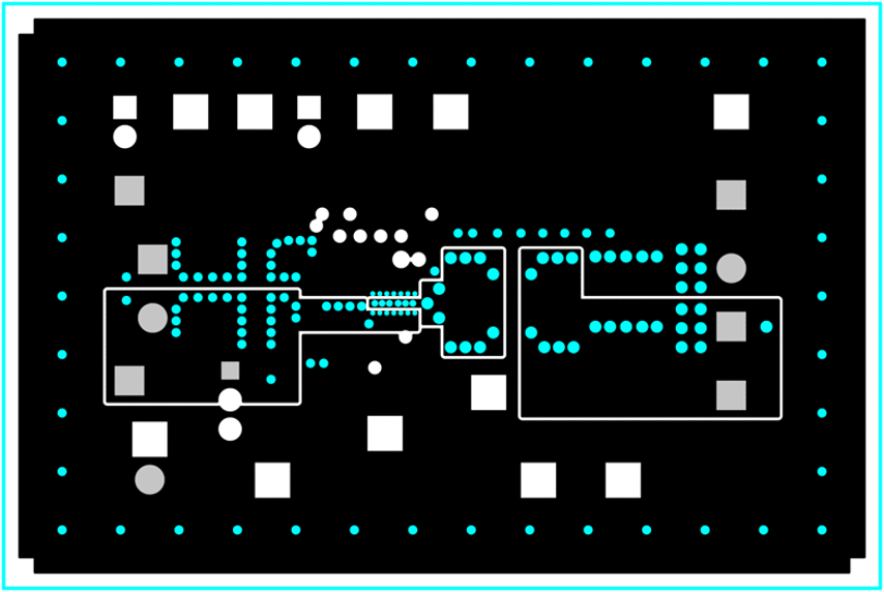 Figure 3-2 TPS54020EVM-082 Internal 1 Copper
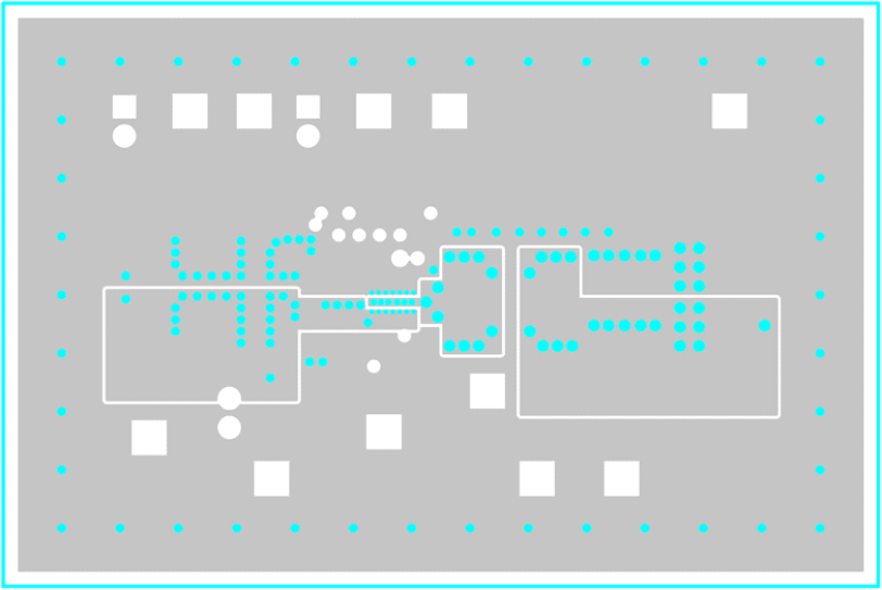 Figure 3-3 TPS54020EVM-082 Internal 2 Copper
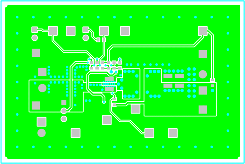 Figure 3-4 TPS54020EVM-082 Bottom Side Copper
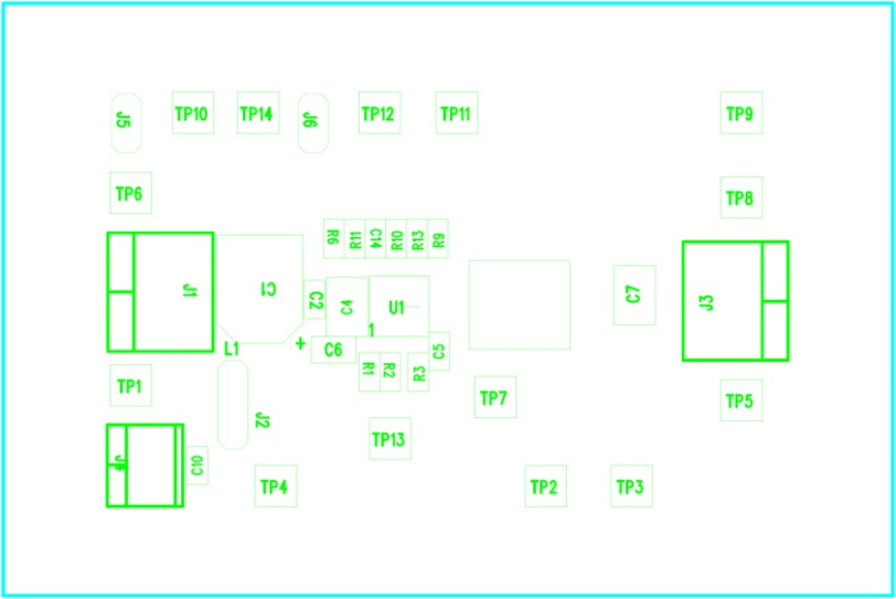 Figure 3-5 TPS54020EVM-082 Top Side Component Placement
 Figure 3-6 TPS54020EVM-082 Bottom Side Component Placement