SLVU777A September   2012  – November 2021 TPS54020


  1.   Trademarks
  2. 1Introduction
    1. 1.1 Background
    2. 1.2 Performance Specification Summary
    3. 1.3 Modifications
      1. 1.3.1 Output Voltage Setpoint
      2. 1.3.2 Slow-Start Time
      3. 1.3.3 Adjustable UVLO
      4. 1.3.4 Input Voltage Rails
  3. 2Test Setup and Results
    1. 2.1  Input / Output Connections
    2. 2.2  Efficiency
    3. 2.3  Output Voltage Load Regulation
    4. 2.4  Output Voltage Line Regulation
    5. 2.5  Load Transient
    6. 2.6  Control Loop Response
    7. 2.7  Output Voltage Ripple
    8. 2.8  Input Voltage Ripple
    9. 2.9  Start Up
    10. 2.10 Pre-Bias Start Up
    11. 2.11 Hiccup Mode Current Limit
  4. 3Board Layout
    1. 3.1 Layout
  5. 4Schematic and Bill of Materials
    1. 4.1 Schematic
    2. 4.2 Bill of Materials
  6. 5Revision History

Control Loop Response

Figure 2-5 shows the EVM control loop response characteristics. Gain and phase plots are shown for VIN voltage of 12 V and a constant resistance load current of 5 A.
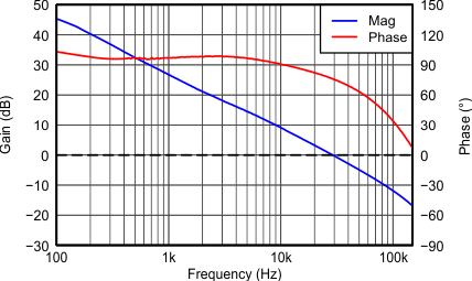
GUID-0D8C93A7-CD09-4BE6-B4B4-9F98A8F17A86-low.gifFigure 2-5 TPS54020EVM-082 Loop Bode Response