SLVUAP8A April 2016 – October 2021 TPS54202H
3.1 Layout
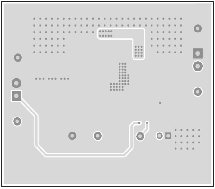
Figure 3-1 and Figure 3-2 show the board layout for the TPS54202HEVM-716. The topside layer of the EVM is laid out in a manner typical of a user application. The top and bottom layers are 2-oz. copper.
The top layer contains the main power traces for VIN, VOUT, and SW. Also on the top layer are connections for the remaining pins of the TPS54202H and a large area filled with ground. To facilitate the placement of the main input bypass capacitor as close to the VIN and GND pins as possible, the trace for SW is routed to the bottom layer immediately at the pin 3 connection. It is routed back to the top layer at the L1 inductor and C4 BOOT capacitor. The bottom layer contains a ground plane plus a copper fill area for SW, an etch run to connect the upper resistor of the voltage set point divider to the regulation point at the J2 output connector, and a trace to connect the upper resistor of the UVLO set point divider network to VIN. The top-side ground areas are connected to the bottom and internal ground planes with multiple vias placed around the board to provide a thermal path from the top-side ground area to the bottom-side and internal ground planes.
The input decoupling capacitors (C2, and C1) and bootstrap capacitor (C4) are all located as close to the IC as possible. In addition, the voltage set-point resistor divider components are also kept close to the IC. For the TPS54202H, an additional input bulk capacitor may be required, depending on the EVM connection to the input supply.
 Figure 3-1 TPS54202HEVM-716 Top-Side Assembly
 Figure 3-2 TPS54202HEVM-716 Bottom-Side Layout