SLVUBT0A June 2020 – January 2021
3.5 Signal Headers
Signal headers are provided for the LDOs, BUCK regulators, and GPIO signals. Headers J13 (LDOs), J12 (BUCKs), and J11 (GPIOs) are placed on the perimeter of the board to enable probing of these signals even when in a stacked configuration.
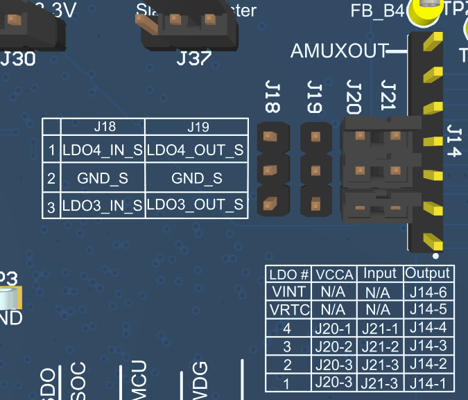
There are 6 signal headers associated with the LDO; five are shown in the EVM silk screen capture, Figure 3-3. These include J20 and J21, the power inputs to the LDOs, J14 and J13, the LDO outputs, and J18 and J19 which can be used to measure Power Supply Rejection Ratio (PSRR) on LDO3 and LDO4. All pins of J20 are connected to the VCCA, and J20 is placed next to J21 to easily connect all the LDO power inputs to the VCCA; this is the default jumper configuration. An external power supply for the LDOs can also be applied directly to J21.
 Figure 3-3 LDO_Headers_v2
Signal Header J12 provides access to all of the buck regulator outputs, GND_S and VCCA_S.
GPIO signals are provided on both J9 and J11. J8 (PU) is located directly above J9 enabling each GPIO to be pulled to the voltage defined in table Table 3-8 through a 10 kΩ resistor pullup. J10 (PD) is located directly below J9 to enable shorting each GPIO directly to GND.
| J8, Pin(s) | Pullup Voltage | Description |
|---|---|---|
| 1,2,7-11 | VIO_IN | GPIO1, GPIO2, GPIO7-11: Output Type Selection; Power Domain is VIO |
| 3,4 | VOUT_LDOVRTC | GPIO3 and GPIO4: Input Type Selection; Power Domain is VRTC |
| 5,6 | VOUT_LDOVINT | GPIO5 and GPIO6: Output Type Selection; Power Domain is VINT |