SLVUBX8B October 2020 – December 2021 TPS2661
- Trademarks
- 1Introduction
- 2Description
- 3Schematic
- 4General Configurations
-
5Test Setup and Procedures
- 5.1 Overload Protection Test
- 5.2 Output Short-Circuit Test
- 5.3 Input Undervoltage Protection Test
- 5.4 Output Undervoltage Protection Test
- 5.5 Output Overvoltage Protection Test
- 5.6 TPS26612 Overload Protection Test
- 5.7 Current Limiting for VIN < –Vs
- 5.8 Surge Protection Test (Current Input, CH1)
- 5.9 Surge Protection Test (Analog Output, CH2)
- 6EVAL Board Assembly Drawings and Layout Guidelines
- 7Bill Of Materials (BoM)
- 8Revision History
6.1 PCB Drawings
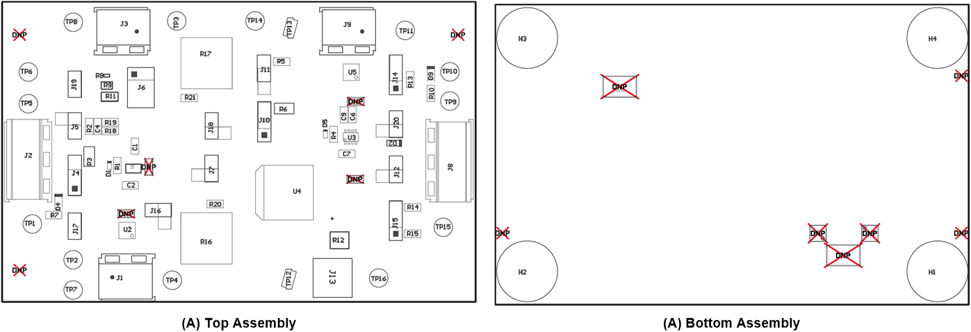
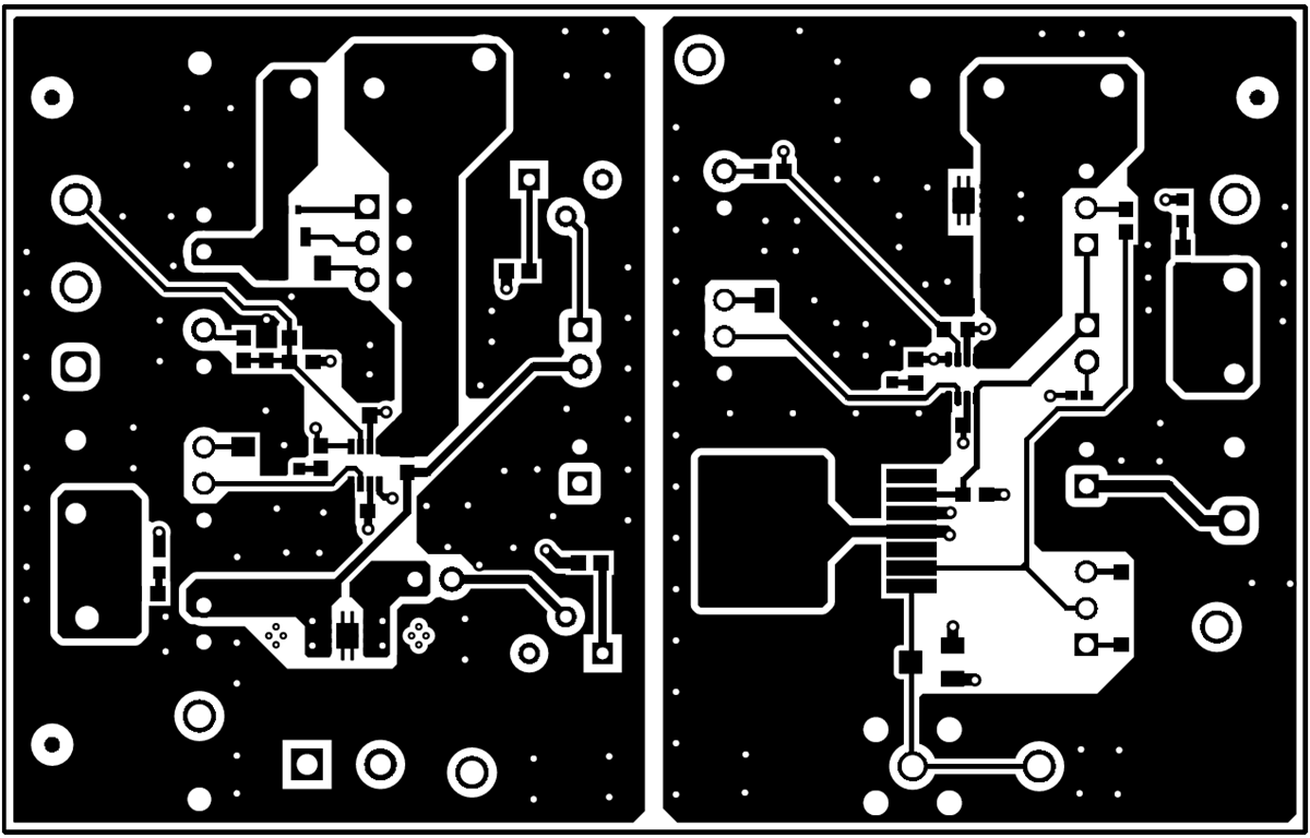
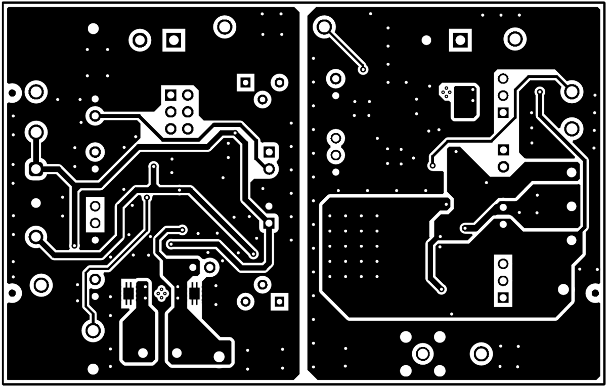
Figure 6-1 shows component placement of the EVAL Board, and Figure 6-2, Figure 6-3 show PCB layout images.
 Figure 6-1 TPS2661EVM Board
Assembly
 Figure 6-2 TPS2661EVM Board Top
Layer
 Figure 6-3 TPS2661EVM Board Bottom
Layer