SLVUBZ6 August 2020 – MONTH
2.3 Layout and Component Placement
Figure 2-2 and Figure 2-3 are the top overlay and bottom overlay of the printed circuit board (PCB) and shows the component placement on the EVM. Figure 2-4 shows the top layout, Figure 2-5 and Figure 2-6 show the top and bottom layers, and Figure 2-7 and Figure 2-8 show the top and bottom solder masks of the EVM.
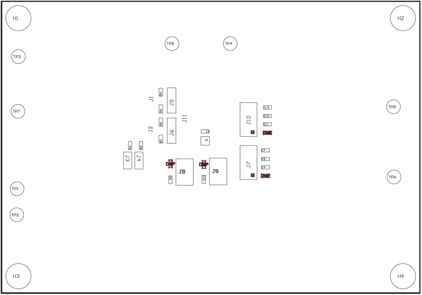 Figure 2-2 Component Placement - Top Overlay
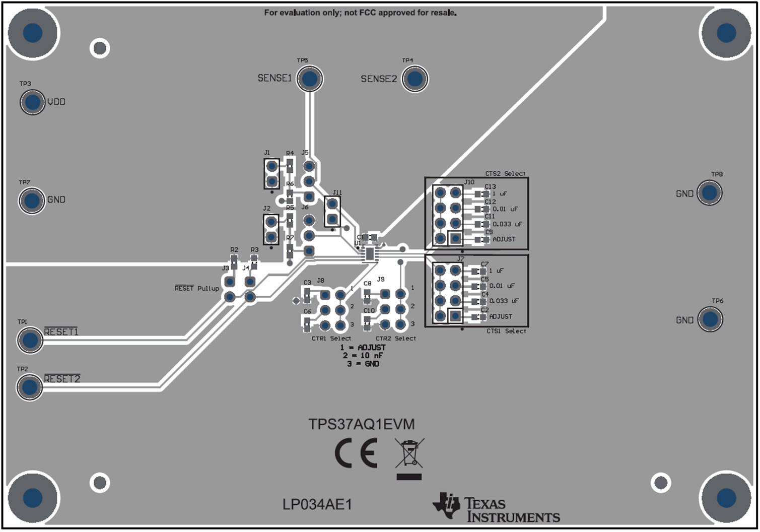 Figure 2-4 Layout - Top
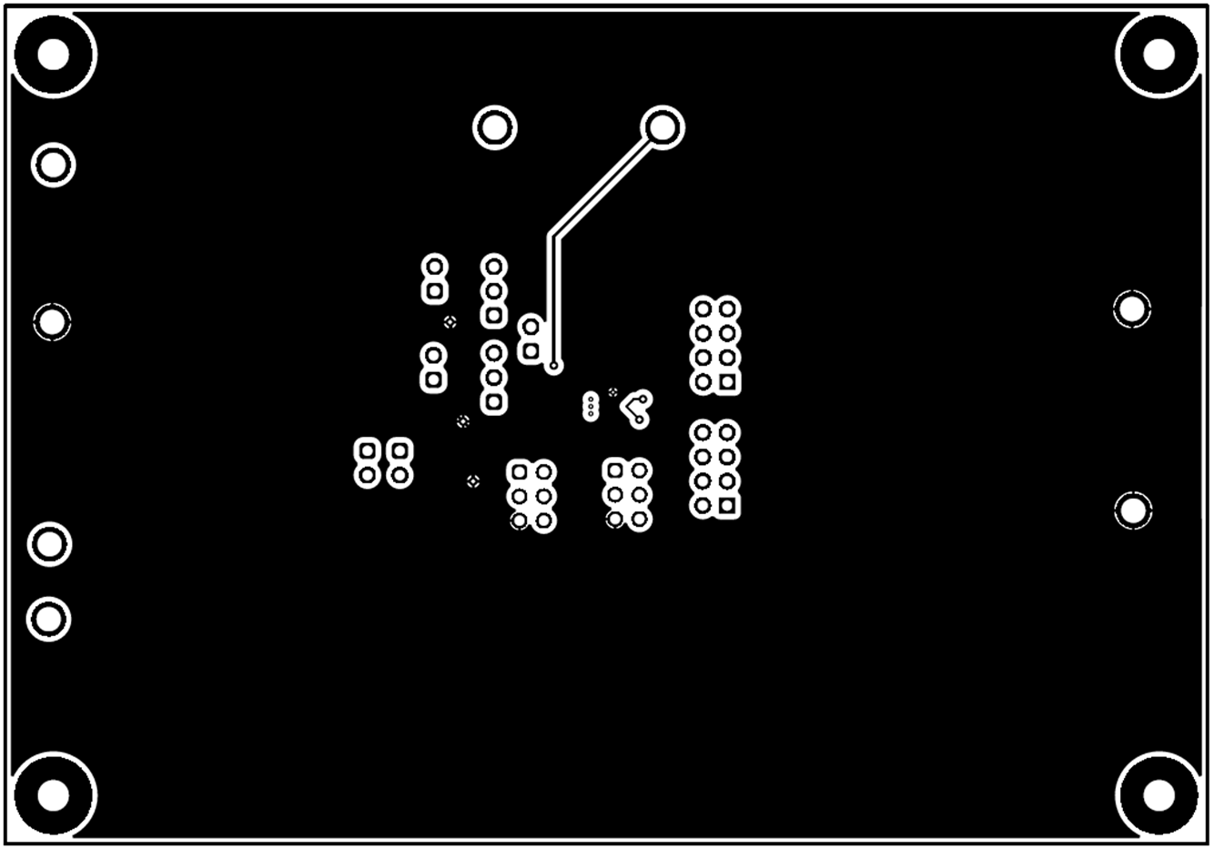 Figure 2-6 Bottom Layer
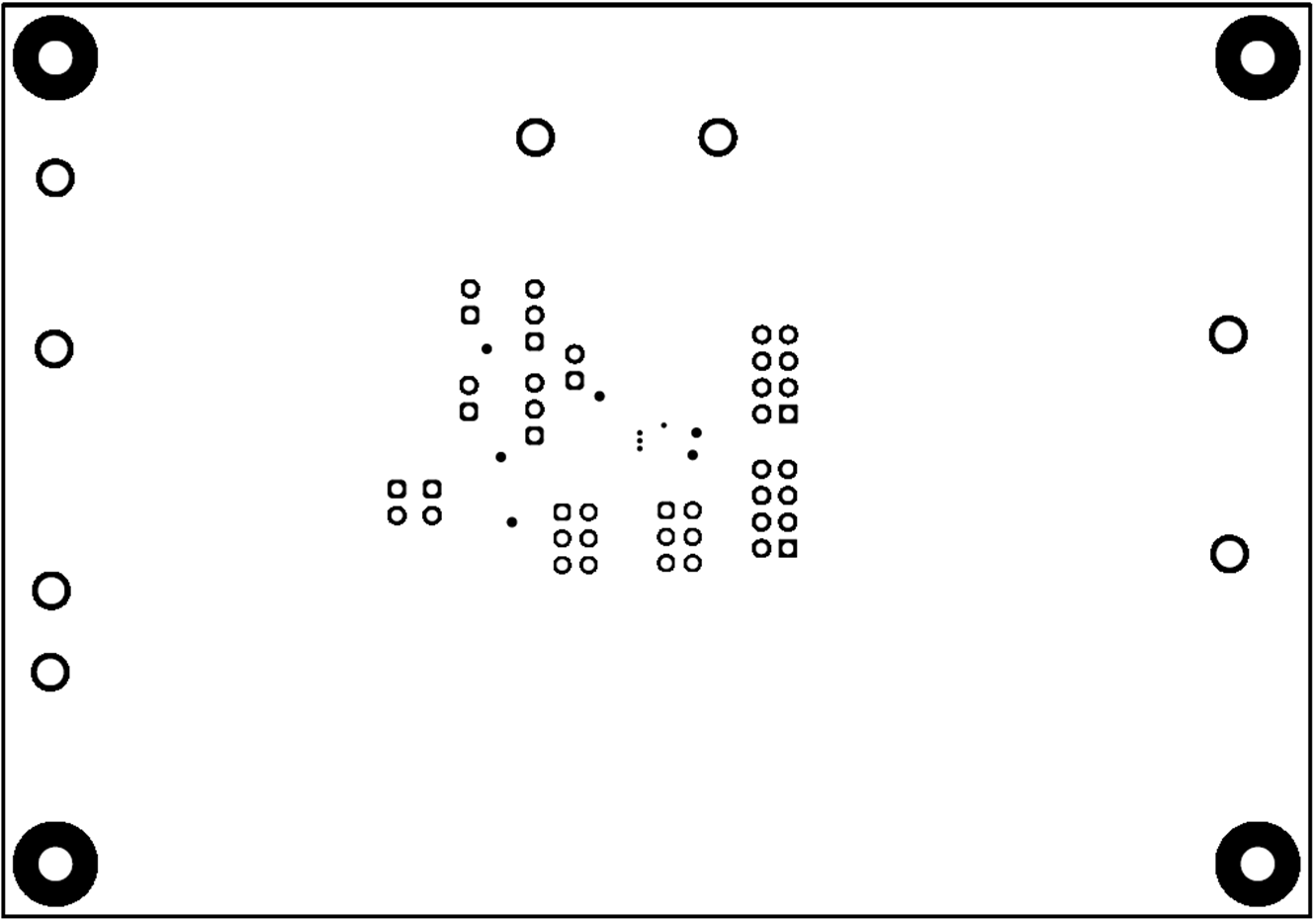 Figure 2-8 Bottom Solder Mask
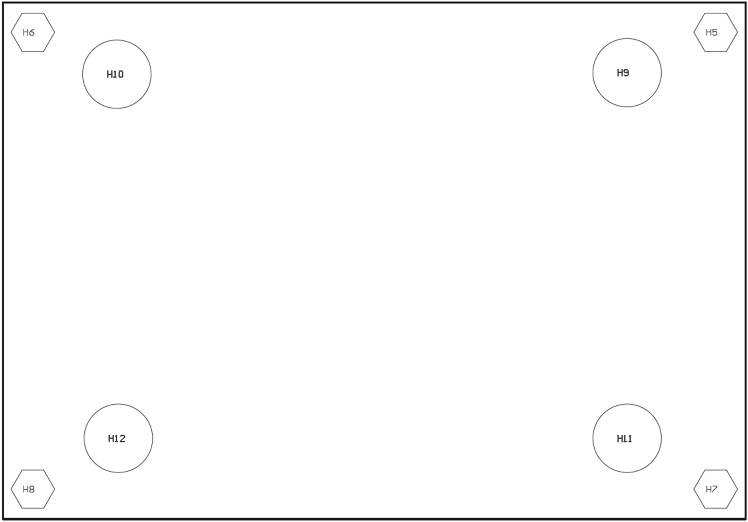 Figure 2-3 Component Placement - Bottom Overlay
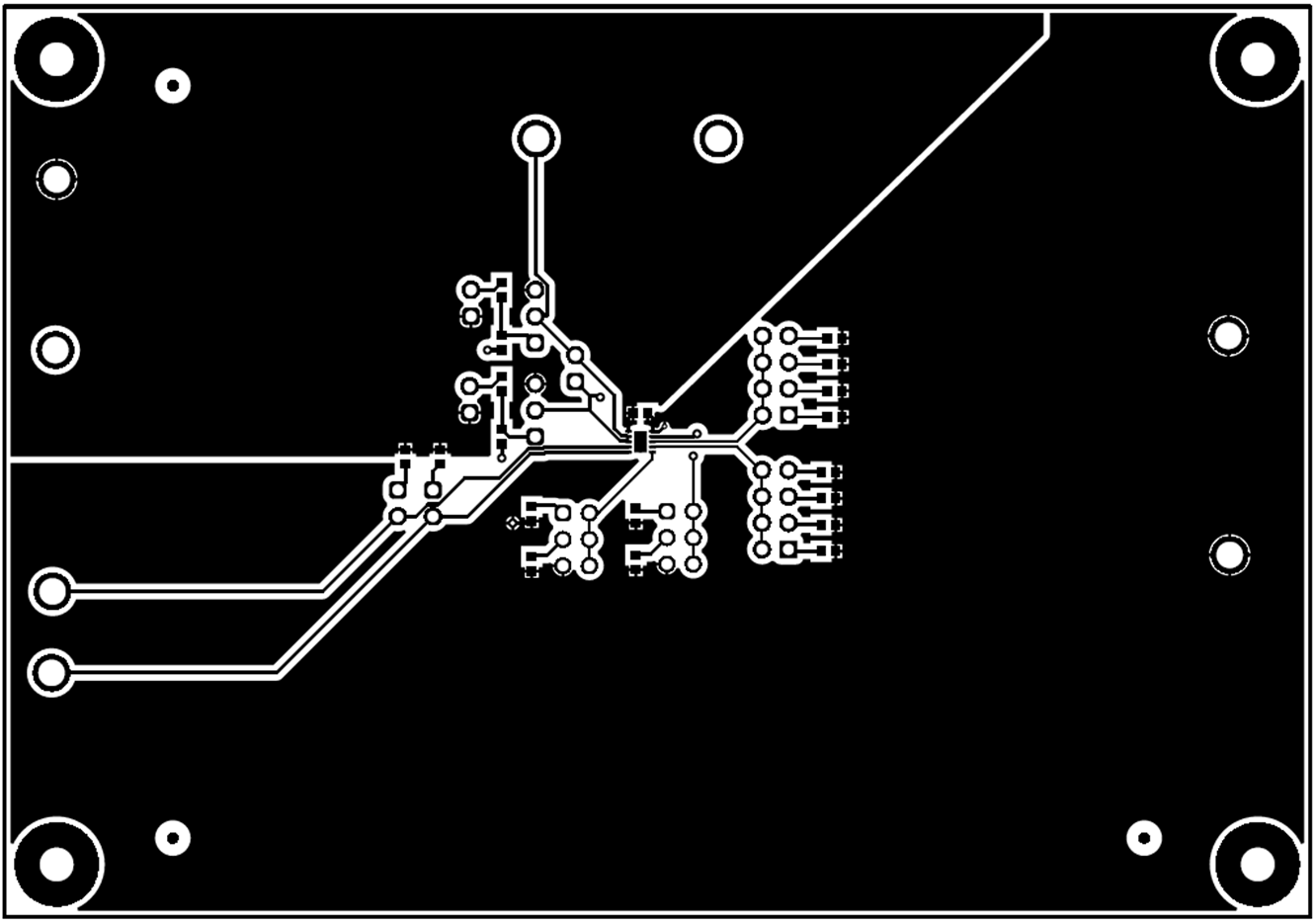 Figure 2-5 Top Layer
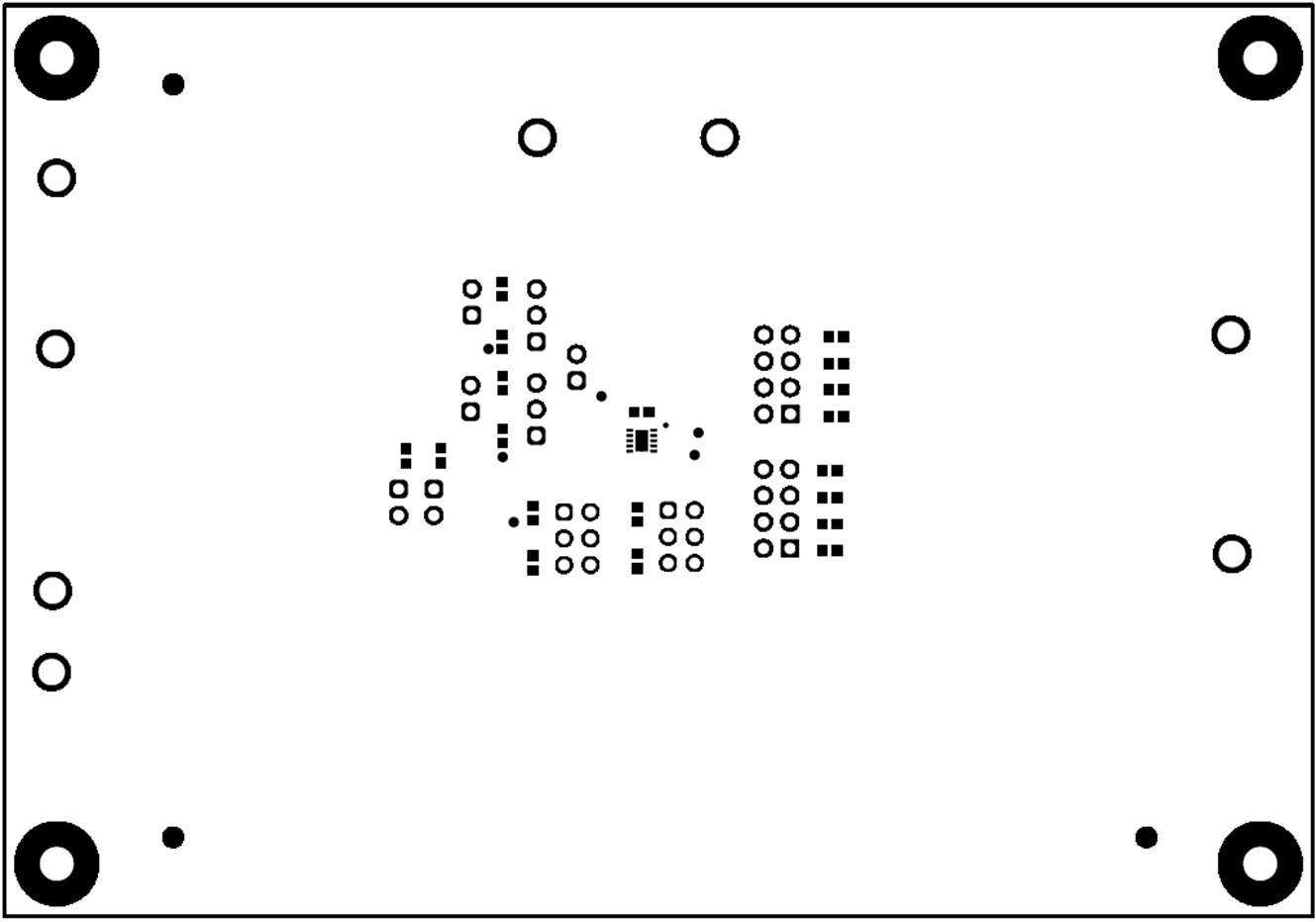 Figure 2-7 Top Solder Mask