SLVUC00 September   2020  – MONTH 


  1. 1Introduction
    1. 1.1 Description
    2. 1.2 Features
  2. 2Electrical Performance
  3. 3Schematic
  4. 4Layout
    1. 4.1 Setup (Channel 1 / Channel 2)
      1. 4.1.1 J1, TP2 / J7, TP8 – Input Connections
      2. 4.1.2 J2, TP4 / J6, TP7 – Output Connections
      3. 4.1.3 J5, TP5 / J10, TP13 – ON
      4. 4.1.4 TP3/TP9 - VIN Sense, TP1/TP6 – VOUT Sense
      5. 4.1.5 J11, TP10 – VBIAS
      6. 4.1.6 J4 / J9 – Output capacitor (Optional)
      7. 4.1.7 TP11, TP12 – GND
  5. 5Operation
  6. 6Test Configurations
    1. 6.1 On-Resistance (RON) Test Setup
    2. 6.2 Rise Time Test Setup
  7. 7Bill of Materials (BOM)

On-Resistance (RON) Test Setup

Figure 6-1 shows the typical setup for measuring on-resistance. Connect the desired VBIAS to the the VBIAS test point. It is recommended that VBIAS is greater than VIN for best on-resistance performance. The voltage drop across the switch is measured using the sense connections, and this can be divided by the load current to calculate the RON resistance.
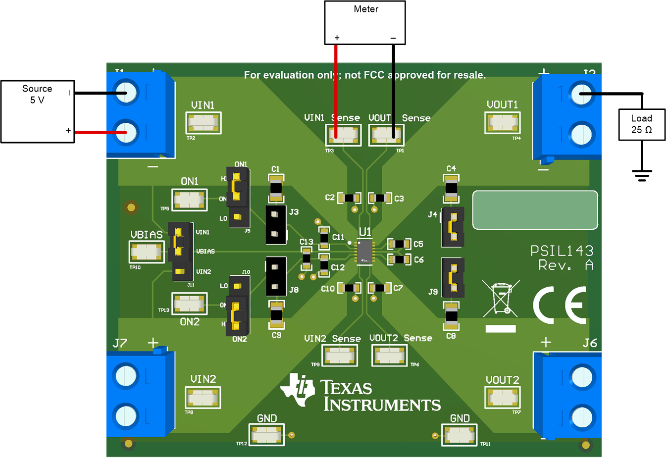
GUID-0837E07F-55CE-47BE-9835-A104C891F6CD-low.png Figure 6-1 RON Test Setup