SLVUC40 May 2021 TPS629210-Q1
5 Test Results
This section provides the test results of TPS629210-Q1EVM.
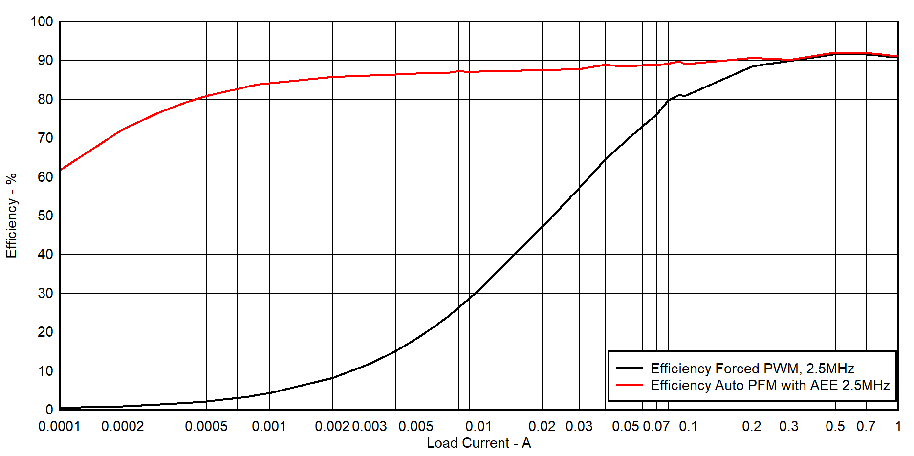 Figure 5-1 Efficiency
VIN= 12 V VOUT = 3.3 V FSW=2.5 MHz
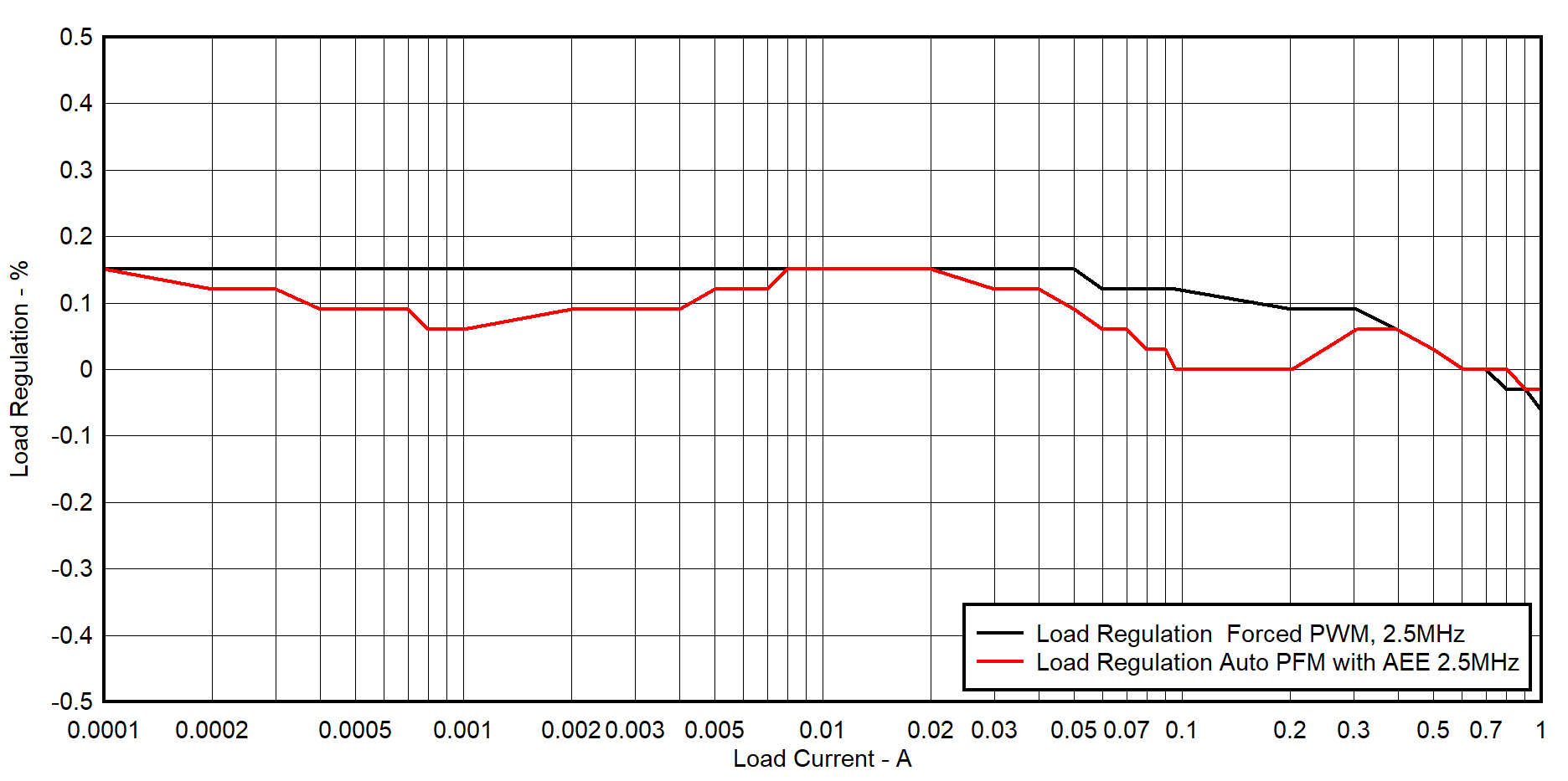 Figure 5-2 Load
Regulation VIN = 12 V VOUT = 3.3 V FSW=2.5 MHz
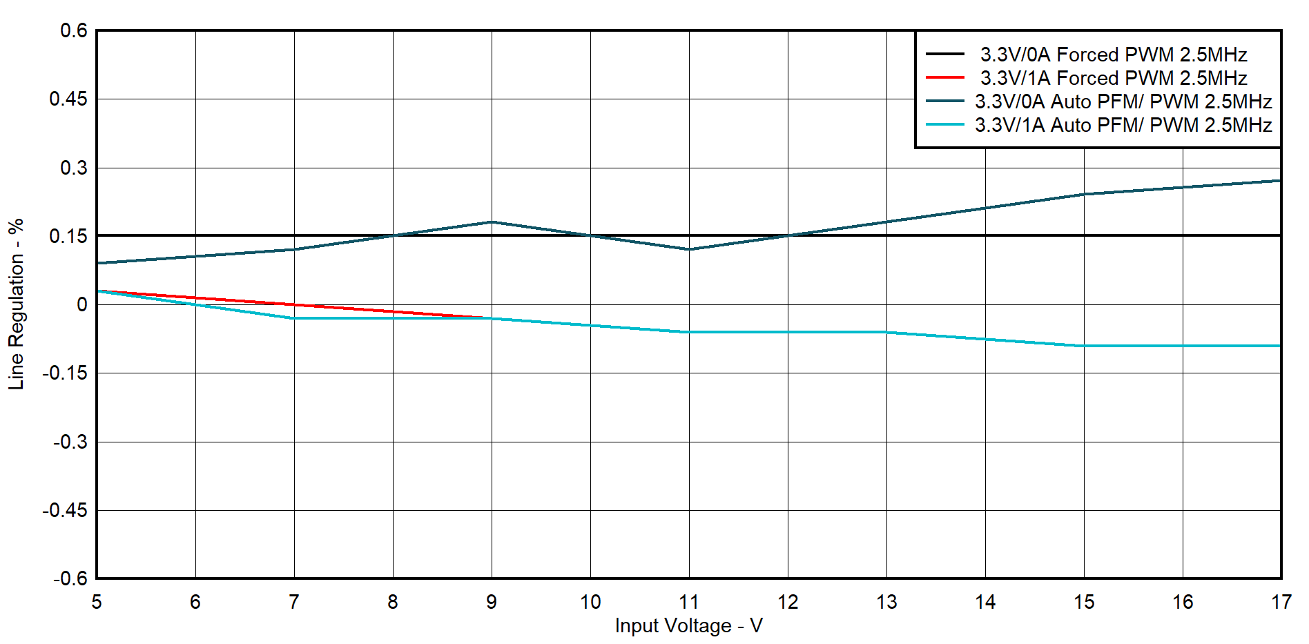 Figure 5-3 Line
Regulation VIN = 5 V–17 V VOUT = 3.3 V IOUT = 0 A and 1
A
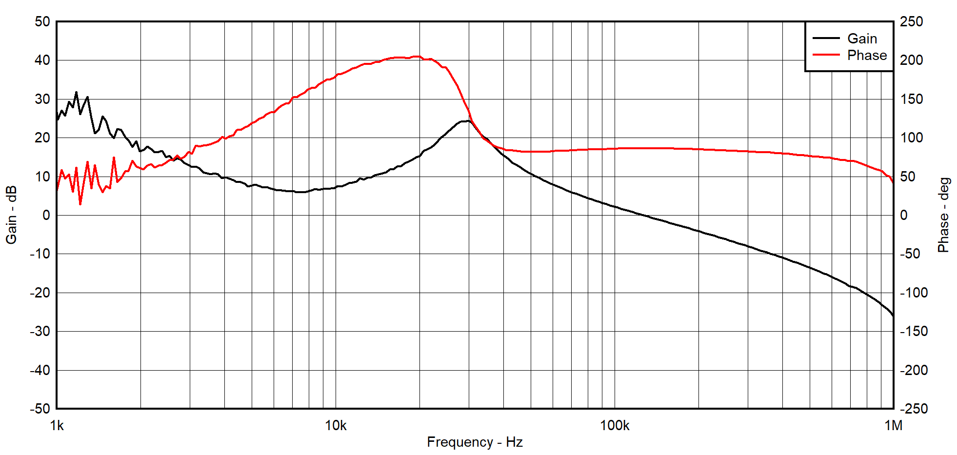 Figure 5-4 Loop
Response Forced PWM Internal FB (VSET) VIN = 12 V VOUT = 3.3 V
IOUT = 1 A
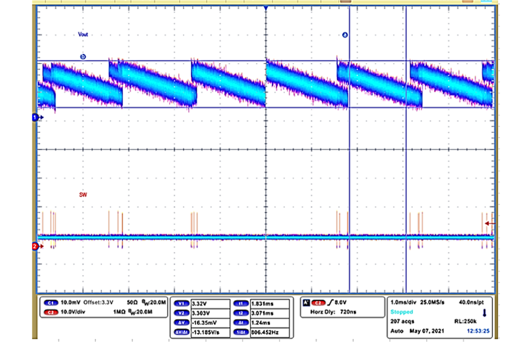 Figure 5-5 Output
Voltage Ripple Auto PFM VIN = 12 V VOUT = 3.3 V IOUT = 0
A
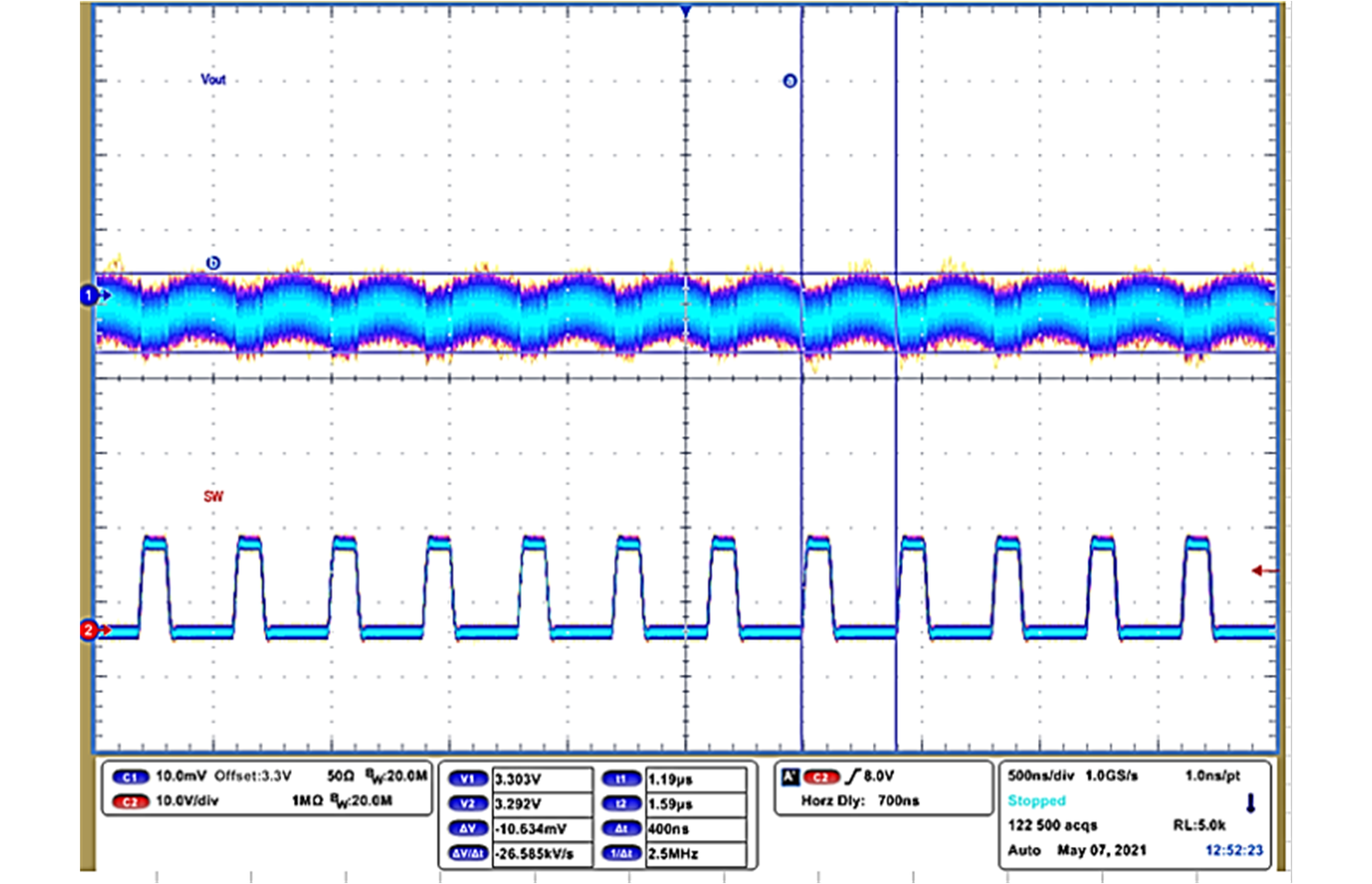 Figure 5-6 Output
Voltage Ripple Forced PWM VIN = 12 V, VOUT = 3.3 V IOUT = 1
A
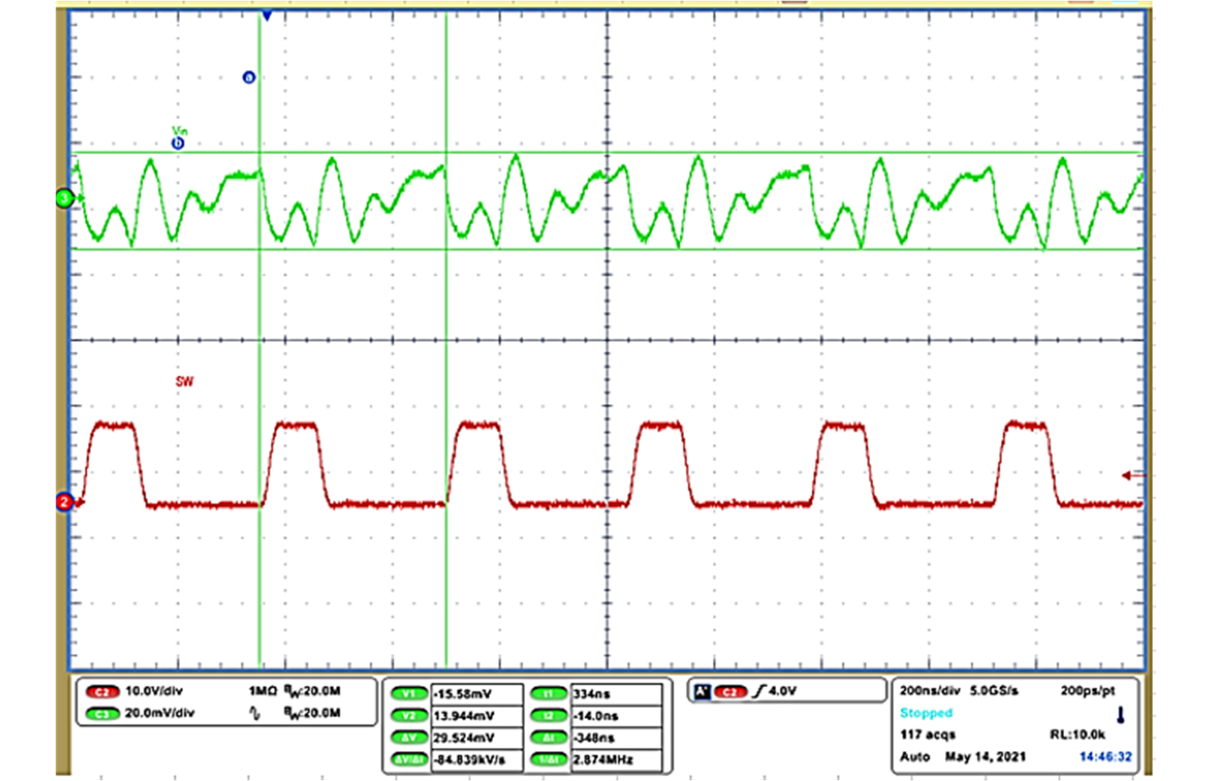 Figure 5-7 Input
Voltage Ripple Forced PWM VIN = 12 V VOUT = 3.3 V IOUT = 1
A
 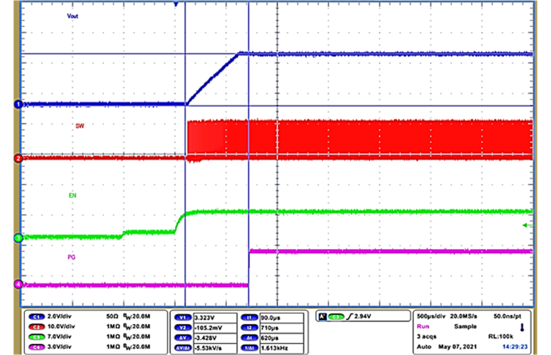 Figure 5-8 Enable
Start Up Forced PWM VIN = 12 V VOUT = 3.3 V IOUT = 1
A
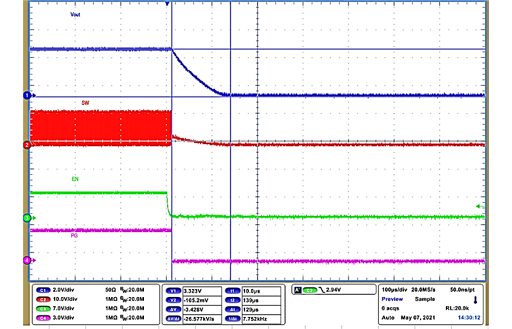 Figure 5-9 Enable
Shutdown Forced PWM VIN = 12 V VOUT = 3.3 V IOUT = 1 A
 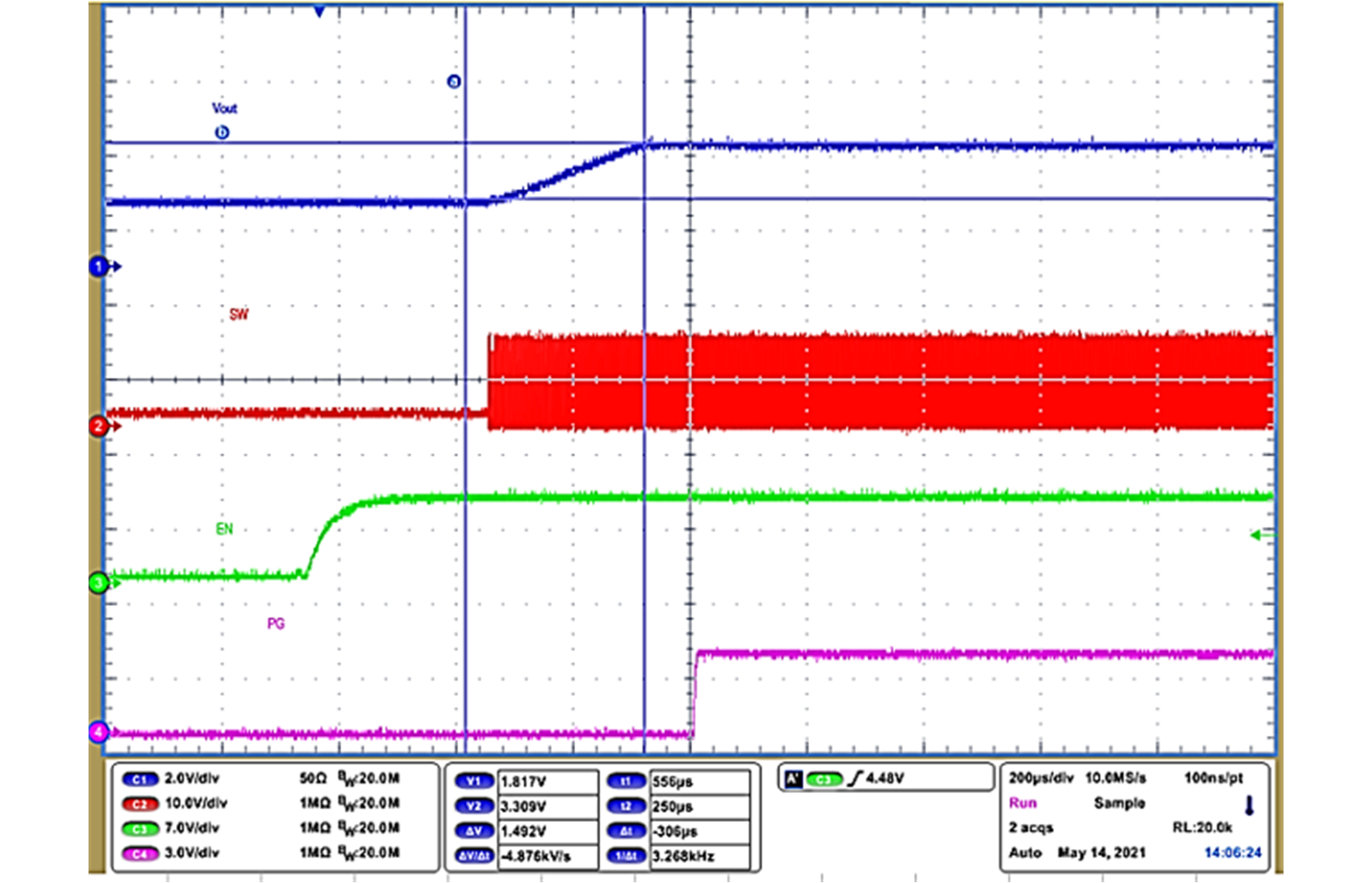 Figure 5-10 Enable
Pre-Bias Start Up Forced PWM VIN = 12 V VOUT = 3.3 V IOUT =
0 A
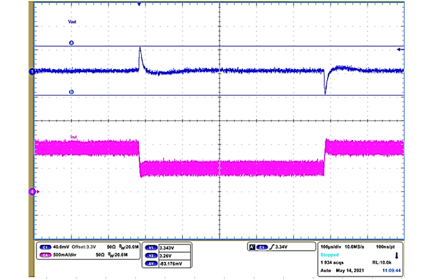 Figure 5-11 Load
Transient Response Forced PWM Internal FB (VSET) VIN = 12 V VOUT = 3.3
V IOUT= 0.5 A–1 A Slew Rate = 1 A/us
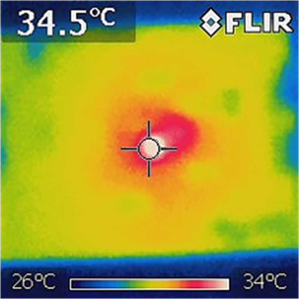 Figure 5-12 Thermal
Performance Forced PWM VIN = 12 V VOUT = 3.3 V IOUT = 1 A
FSW=2.5 MHz