SLVUCC9 September 2022 TLV61070A
4 Board Layout
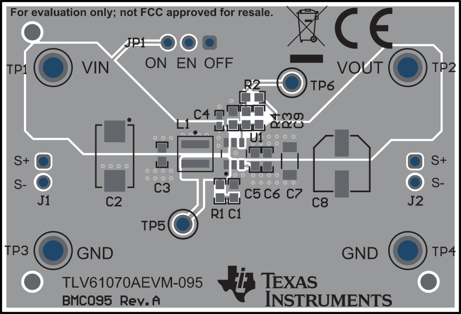
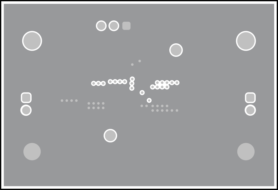
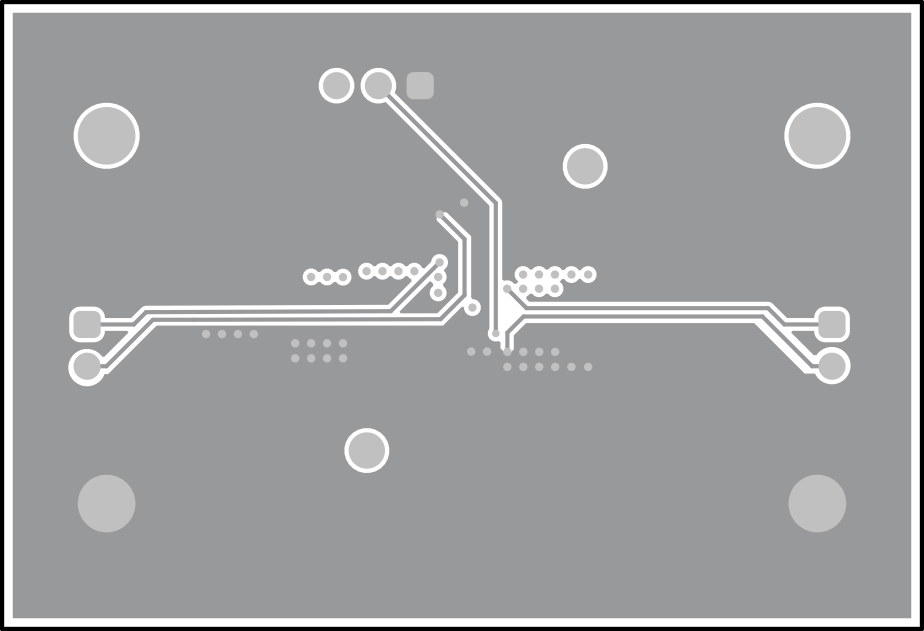
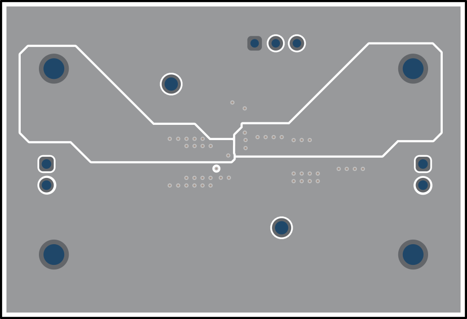
The PCB of the TLV61070AEVM has four layers. Figure 4-1 and Figure 4-4 illustrate top and bottom side PCB layout. The two inner layers are ground plane helping improve the thermal performance.
 Figure 4-1 TLV61070AEVM-095 Top-Side Layout
 Figure 4-2 TLV61070AEVM-095 Inner Layer 1 Layout
 Figure 4-3 TLV61070AEVM-095 Inner Layer 2 Layout
 Figure 4-4 TLV61070AEVM-095 Bottom-Side Layout